Switching converter control circuit

Active Publication Date: 2011-10-06
TEXAS INSTR INC
View PDF12 Cites 16 Cited by
  • Summary
  • Abstract
  • Description
  • Claims
  • Application Information

AI Technical Summary

Benefits of technology

[0006]A DC-DC converter with one aspect of the inventive control circuit does not need a very low offset and high speed comparator. Only a less accurate helper comparator is needed with reduced requirements of silicon area on the chip since the comparator monitors a large high or low excursion on the switching node following the low-side transistor tur

Problems solved by technology

While this solution is very effective at high load currents, a problem at low load current is that the inductor current reverses and will not be blocked naturally by reverse biasing of a diode.
This results in a power loss in the synchronous rectifier, reducing efficiency at low load current.
However, a low-offset high speed comparator is needed for this approach.
At low load current, the voltage drop across the transistor is extremely small, typically in a single-digit mV range, making exorbitant demands on the comparator in terms of accuracy and speed.

Method used


Image

  • Switching converter control circuit
  • Switching converter control circuit
  • Switching converter control circuit

Examples


Embodiment Construction

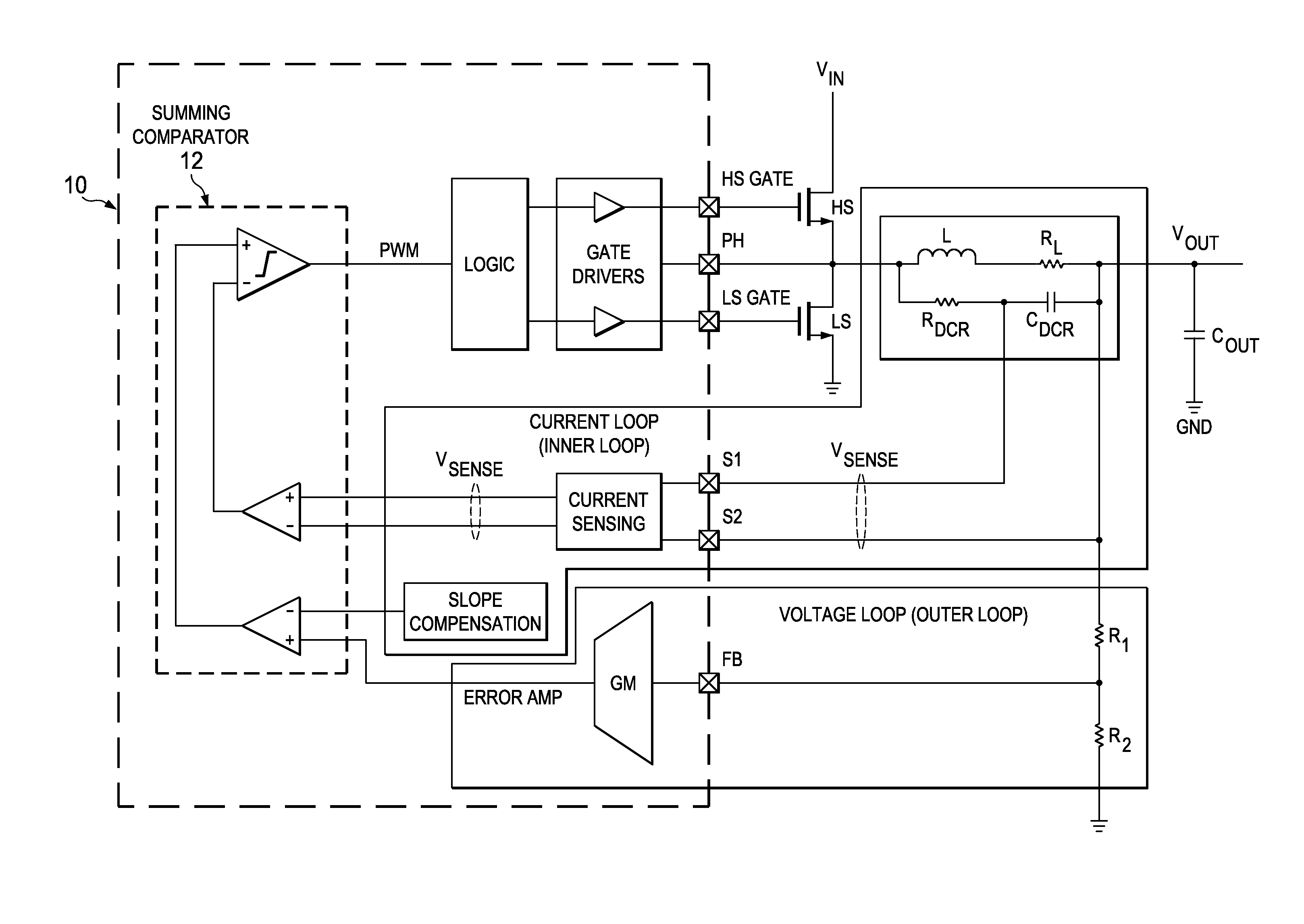
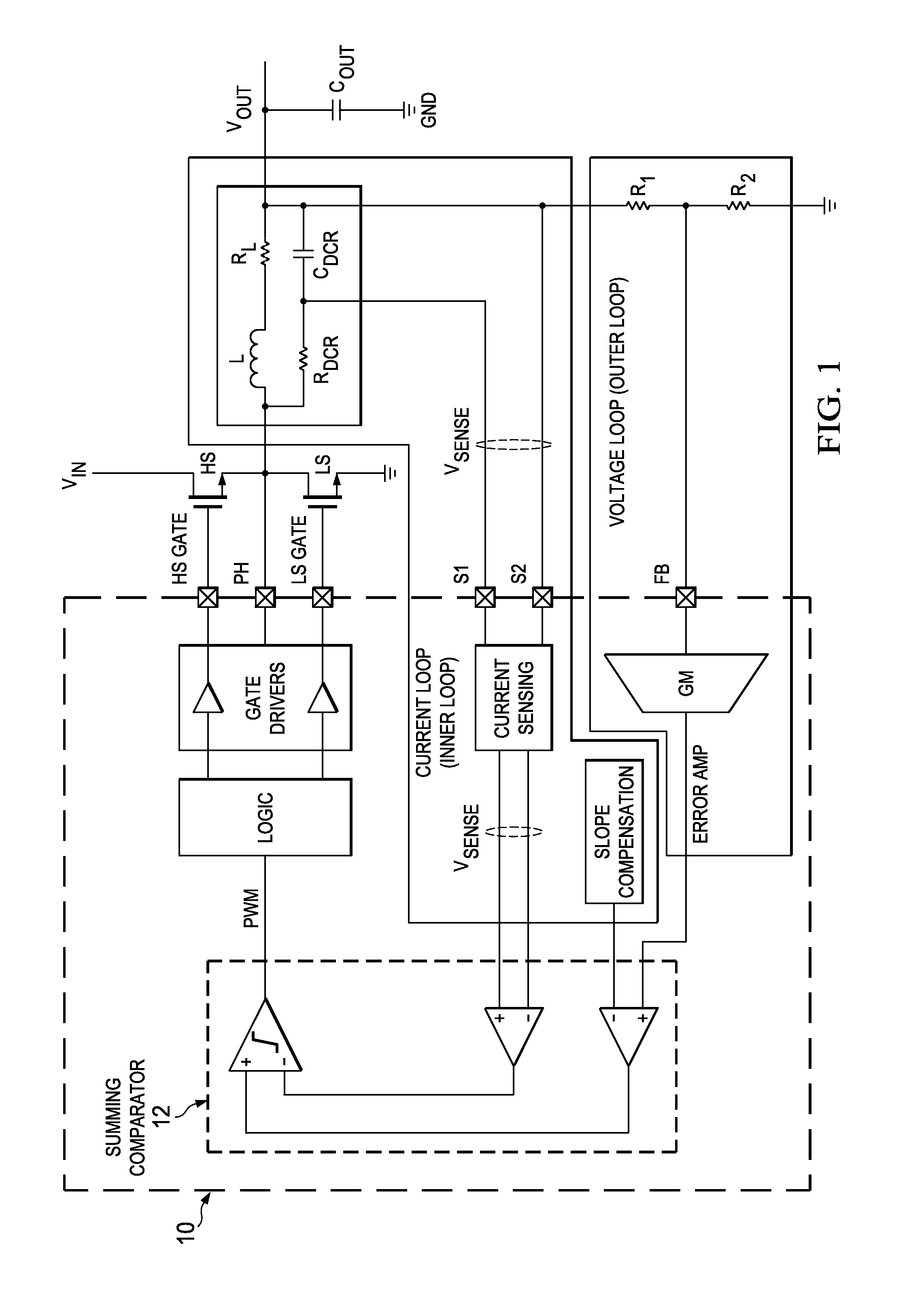
[0017]The example embodiment disclosed is a buck converter, it being understood that the principles of the invention are applicable generally to switched mode power supplies and, of course, to boost converters, with only minor modifications.

[0018]In FIG. 1, block 10 is an integrated control circuit incorporating the control logic and gate drivers for external power MOSFET transistors, high-side transistor HS and low-side transistor LS, connected in series between supply terminal VIN and ground GND. The interconnection node PH of both transistors, the converter's switching node, is connected to the converter's output VOUT through an inductor L as is conventional. Also shown is a parasitic resistive component RL of the inductor. The output VOUT is buffered with a capacitor COUT as usual. The control circuit includes analog control circuitry in a block 12 with a summing comparator that provides a pulse width modulated signal PWM to the control logic and inputs from a current sensing ci...


PUM


Abstract

A DC-DC converter has a control circuit for controlling a high-side power transistor and a low-side power transistor connected in series between supply terminals to which an input supply voltage is applied. The converter has a switching node at the interconnection of the power transistors for connection of an inductor to which a load is connected. The control circuit has a feedback loop that provides a pulse width modulated control signal, logic circuitry to which the pulse width modulated control signal is applied and gate drivers with inputs connected to outputs of the logic circuitry and outputs applying gate drive signals to the gates of the power transistors. A digital signal is obtained which is indicative of whether the converter switching node is at a potential above or below a zero reference at the time of the turn-off edge of the low-side gate drive signal. The turn-off edge of the low-side gate drive signal is advanced or delayed by a predetermined amount in response to the value of the digital signal.

Description

CROSS-REFERENCE TO RELATED APPLICATIONS[0001]This application is claims priority from German Patent Application No. 10 2010 013 353.1, filed Mar. 30, 2010, which is hereby incorporated by reference for all purposes.FIELD OF THE INVENTION[0002]The invention relates to a DC-DC converter control circuit for controlling the high-side and low-side power transistors connected in series between supply terminals.BACKGROUND OF THE INVENTION[0003]A typical DC-DC converter has a high-side power transistor and a low-side power transistor connected in series between supply terminals, and an external inductor connected between the interconnection node of the power transistors, usually referred to as the switch node, and an output terminal to which a load is connected. The low-side transistor acts as a synchronous rectifier to improve efficiency compared to solutions with a rectifier diode by eliminating the voltage drop across the diode and replacing it with a small voltage drop of a low resistan...

Claims


Application Information

Patent Timeline
IPC IPC(8): G05F1/565
CPCH02M3/157Y02B70/1466H02M3/1588Y02B70/10
Inventor HERZER, STEFANKULKAMI, SUMEET P.NEIDHARDT, JOCHEN
Owner TEXAS INSTR INC
Why Eureka
Try Eureka