High efficiency bi-directional charge pump circuit

a charge pump and bi-directional technology, applied in the field of integrated circuits, can solve the problems of limiting the number of stages that can be effectively cascaded, the need for thick oxide (high voltage) transistors to withstand the large potential differences between gate and bulk terminal, and the reliability would be compromised, so as to achieve high efficiency, simplify implementation, and boost both positive and negative potentials

Inactive Publication Date: 2006-12-07
ATMEL CORP
View PDF24 Cites 19 Cited by
  • Summary
  • Abstract
  • Description
  • Claims
  • Application Information

AI Technical Summary

Benefits of technology

[0008] The present invention is an apparatus and method for a voltage charge pump which solves the problems inherent in the prior art. A charge pump, fabricated in a standard CMOS process on a p-type substrate utilizing a triple-well NMOS transistor structure, with high efficiency and capability of boosting both positive and negative potentials is introduced in the present invention. The charge pump requires only thin oxide (low voltage) transistors, simplifying implementation and expanding the opportunity for its application in a variety of process technologies. The present invention reduces the silicon area requirement in a Flash memory by providing a source of both elevated positive and negative voltages with a single circuit. Furthermore, the present invention can be applied to other applications and circuits where elevated voltages are required.

Problems solved by technology

Moreover, the well-known body effect increases the effective threshold voltage of the NMOS devices as the potential between the source and bulk terminals increases, thereby limiting the number of stages that can be effectively cascaded.
Another drawback of the prior art charge pump is that thick oxide (high voltage) transistors are required to withstand the large potential differences developed between the gate and bulk terminals.
Without the use of thick oxide devices, reliability would be compromised.
The necessity for thick oxide transistors makes design with standard thin oxide (low voltage) transistors impossible, adding to process complexity and cost.
Finally, the circuit should not require special device configurations (thick oxide, or PMOS triple well) which necessitate additional fabrication complexity and increased cost.

Method used


Image

  • High efficiency bi-directional charge pump circuit
  • High efficiency bi-directional charge pump circuit
  • High efficiency bi-directional charge pump circuit

Examples


Embodiment Construction

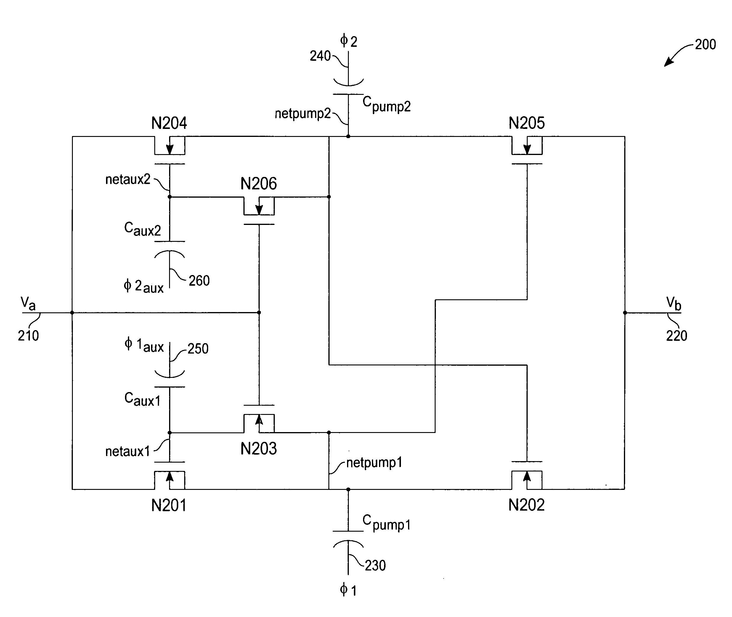
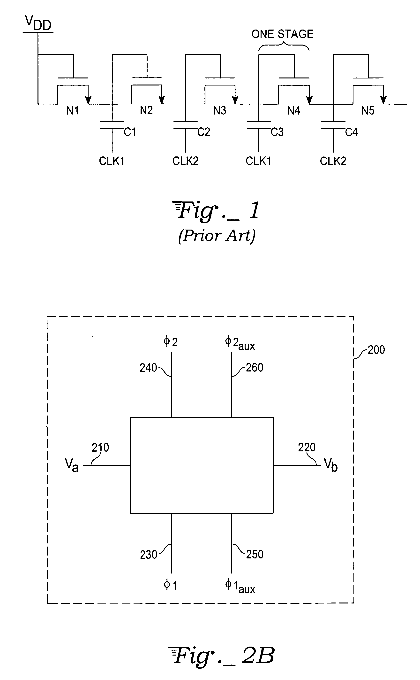
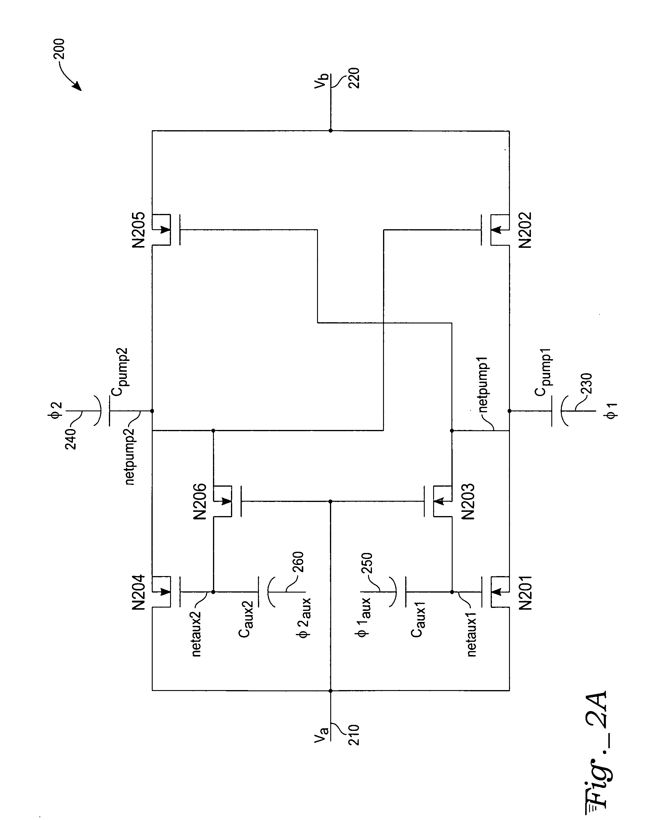
[0015] With reference to FIG. 2A, a charge pump stage 200 according to an exemplary embodiment of the present invention comprises a first voltage input / output node 210 associated with a potential Va, a second voltage input / output node 220 associated with a potential Vb, a first control clock node 230 associated with a clock signal φ1, a second control clock node 240 associated with a clock signal φ2, a first auxiliary control clock node 250 associated with a clock signal φ1aux, and a second auxiliary control clock node 260 associated with a clock signal φ2aux. The charge pump stage 200 further comprises NMOS transistors N201-N206. In an exemplary embodiment of the present invention, the NMOS transistors N201-N206 are low-voltage devices, each implemented within a triple-well structure. The methods of fabricating triple-well NMOS transistors are well known to those skilled in the art and will not be articulated here to avoid obscuring the present invention. Skilled artisans will appr...


PUM


Abstract

A charge pump circuit having a first voltage node acting as an input when the charge pump circuit boosts negative voltages, and acting as an output when the charge pump circuit boosts positive voltages and a second voltage node acting as an input when the charge pump circuit boosts positive voltages, and acting as an output when the charge pump circuit boosts negative voltages. The charge pump circuit further has a first pump capacitor, a second pump capacitor, a first auxiliary capacitor, and a second auxiliary capacitor.

Description

TECHNICAL FIELD [0001] The present invention is related to integrated circuits. More specifically, the present invention is an apparatus and method for a voltage charge pump circuit. BACKGROUND ART [0002] Charge pump circuits are commonly used to provide high positive and negative voltages in applications such as programming of Flash memories. The conventional approach is to employ separate charge pump circuits, one for the generation of positive voltage, and another for the generation of negative voltage. Typical charge pump circuits comprise a significant portion of the silicon area of a Flash memory circuit. If high positive and negative voltages are not simultaneously required, a reversible, bi-directional charge pump capable of generating both positive and negative voltages becomes an attractive opportunity to provide area and cost savings. [0003] A popular approach to the creation of a voltage charge pump in the prior art is embodied in an architecture known as the Dickson cha...

Claims


Application Information

Patent Timeline
Patent Type & Authority Applications(United States)
IPC IPC(8): G05F1/10
CPCH02M3/073G11C16/30
Inventor DAGA, JEAN-MICHELRACAPE, EMMANUEL
Owner ATMEL CORP
Why Eureka
Try Eureka