Defect classification method and apparatus, and defect inspection apparatus

Inactive Publication Date: 2008-03-27
HITACHI HIGH-TECH CORP
View PDF3 Cites 65 Cited by
  • Summary
  • Abstract
  • Description
  • Claims
  • Application Information

AI Technical Summary

Benefits of technology

[0007]The defect sort of the rule base type has an advantage that classify condition setting with a user's intention reflected therein on the basis of the theory and experience is possible and the user can easily understa

Problems solved by technology

However, the defect classify of the rule base type has a problem that it is difficult to set all of the classify condition manually if feature kinds or defect class kinds have in

Method used


Image

  • Defect classification method and apparatus, and defect inspection apparatus
  • Defect classification method and apparatus, and defect inspection apparatus
  • Defect classification method and apparatus, and defect inspection apparatus

Examples


first embodiment

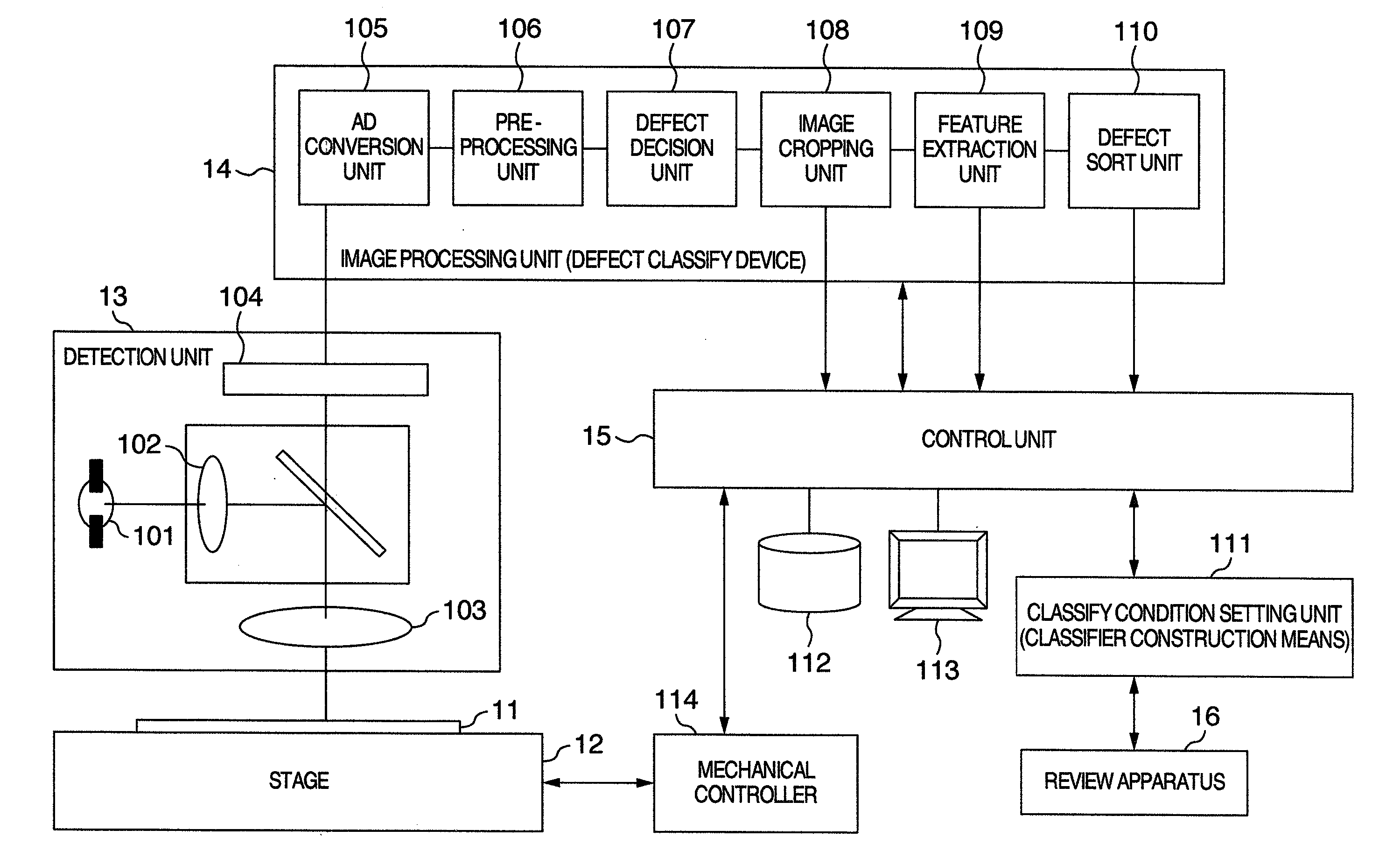
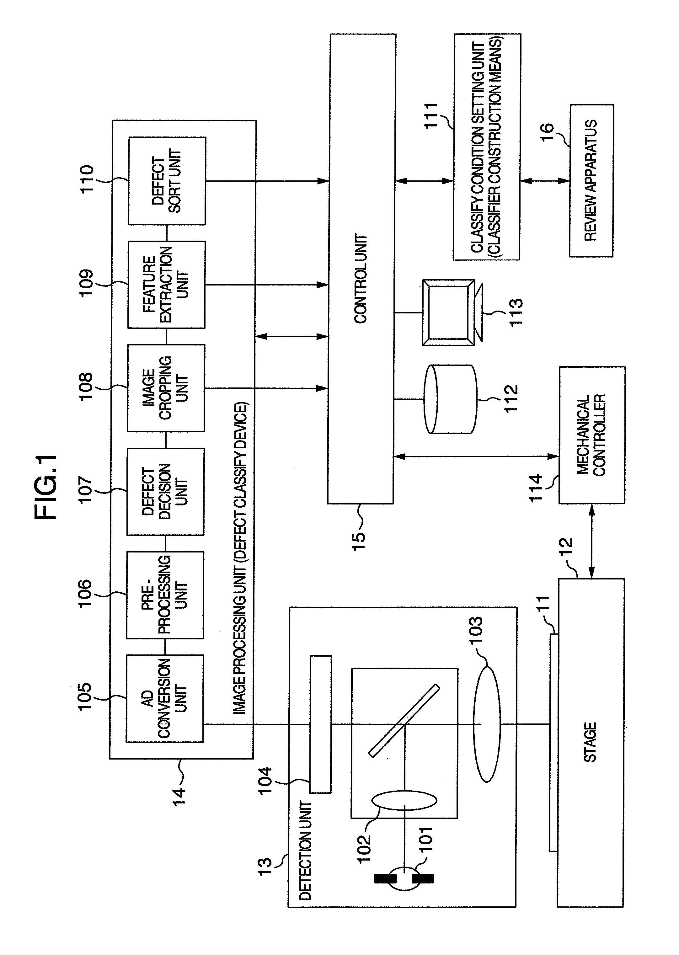
[0042]The first embodiment of a defect classification method, and apparatus, and a defect inspection method, and apparatus, in which defects are classified by using a classifier constructed (generated) with a classify condition setting function according to the present invention will be described in detail with reference to FIGS. 1 to 15.

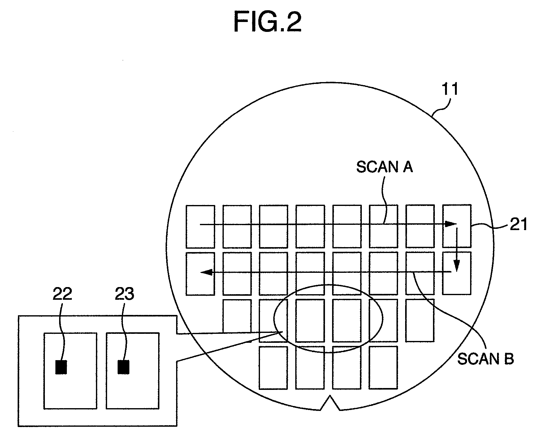
[0043]As the first embodiment, the case of an optical defect inspection apparatus (optical visual inspection apparatus) for semiconductor wafers will be described. FIG. 1 shows an embodiment of a configuration of the optical defect inspection apparatus. The first embodiment is not restricted to optical defect inspection apparatuses, but is applicable to electron beam type defect inspection apparatuses or the like, as well. Reference numeral 11 denotes an inspection subject such as a semiconductor wafer. Reference numeral 12 denotes a stage for mounting and moving the inspection subject 11. Reference numeral 13 denotes a detection unit. The detection...

second embodiment

[0081]A second embodiment of a defect classification method, and apparatus, and a defect inspection method, and apparatus, in which defects are classified by using a classifier constructed (generated) with a classify condition setting function according to the present invention will be described in detail with reference to FIGS. 16 to 22.

[0082]The second embodiment according to the present invention differs from the first embodiment in that the second embodiment has a function of specifying user's intention (target performance of purity and accuracy for each defect class, the whole and the worst case) with a priority order and a function of evaluating performance of sort according to the preset sort condition and displaying whether the specified target performance is satisfied, for each item intended by the user.

[0083]The defect inspection apparatus (visual inspection apparatus) according to the second embodiment has a configuration similar to that of the first embodiment. By the wa...


PUM


Abstract

A defect classification method to classify defects by using a classifier having a binary tree structure based on features of defects extracted from detected signals acquired from a defect inspection apparatus includes a classifier construction process for constructing the classifier by setting a branch condition including defect classes respectively belonging to groups located on both sides of the branch point, a feature to be used for branching, and a discriminant reference, for each branch point in the structure based on instruction of defect classes and feature data respectively associated therewith beforehand. The process includes a priority order specification process for previously specifying target classification performance of purity and accuracy for each defect class, whole and in worst case, with priority order, and an evaluation process for evaluating whether the specified target classification performance under the branching condition is satisfied and displaying a result of evaluation, every item.

Description

INCORPORATION BY REFERENCE[0001]The present application claims priority from Japanese application JP2006-262083 filed on Sep. 27, 2006, the content of which is hereby incorporated by reference into this application.BACKGROUND OF THE INVENTION[0002]The present invention relates to a defect classify and inspection method, and apparatus, to classify defects such as minute pattern defects and dust particles on the basis of an image of an inspection subject obtained from a thin film device such as a semiconductor wafer, a TFT or a photomask by using lamp light, laser light or an electron beam. In particular, the present invention relates to a defect inspection method, and apparatus, suitable for inspecting defects in a semiconductor wafer.[0003]Thin film devices such as semiconductor wafers, liquid crystal displays and hard disk magnetic heads are manufactured through a large number of working processes. In the manufacture of such thin film devices, visual inspection is executed every so...

Claims


Application Information

Patent Timeline
IPC IPC(8): G06K9/00G06V10/764G06V10/98
CPCG01N21/9501G01N21/956G06T7/0004G06K9/6254G06K9/6282G06K9/03G06T2207/30148G06V10/98G06V10/764G06V10/7788G06F18/24323G06F18/41
Inventor SHIBUYA, HISAEMAEDA, SHUNJIHAMAMATSU, AKIRA
Owner HITACHI HIGH-TECH CORP
Why Eureka
Try Eureka