Method of Forming A Metallic Oxide Film Using Atomic Layer Deposition

Inactive Publication Date: 2008-03-27
SAMSUNG ELECTRONICS CO LTD
View PDF14 Cites 431 Cited by
  • Summary
  • Abstract
  • Description
  • Claims
  • Application Information

AI Technical Summary

Problems solved by technology

However, the ALD has a slow rate of deposition as comp

Method used


Image

  • Method of Forming A Metallic Oxide Film Using Atomic Layer Deposition
  • Method of Forming A Metallic Oxide Film Using Atomic Layer Deposition
  • Method of Forming A Metallic Oxide Film Using Atomic Layer Deposition

Examples


Embodiment Construction

[0017]Features of the present invention and methods of accomplishing the same may be understood more readily by reference to the following detailed description of preferred embodiments and the accompanying drawings. The present invention may, however, be embodied in many different forms and should not be construed as being limited to the embodiments set forth herein. Like reference numerals refer to like elements throughout the specification.

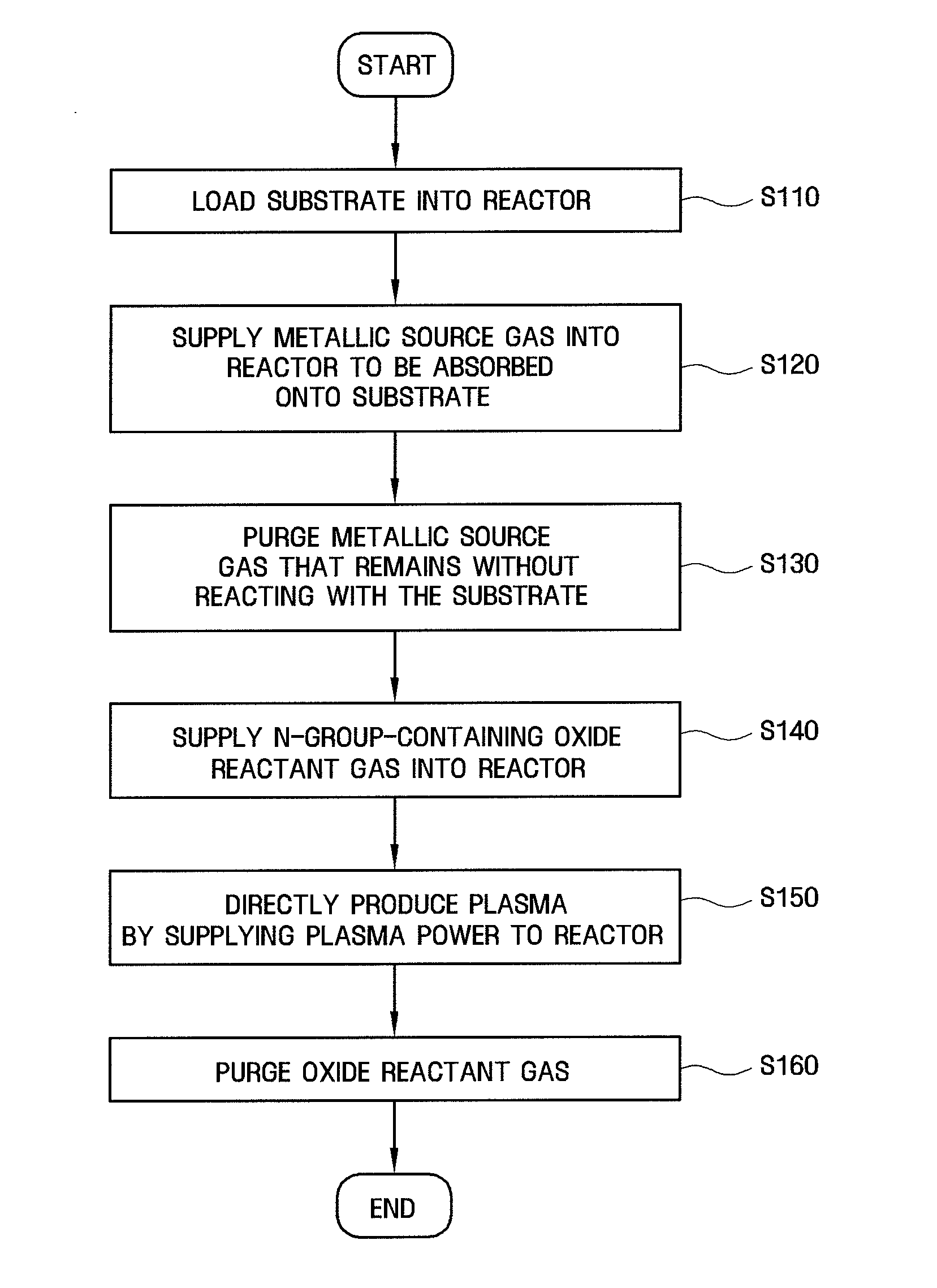
[0018]A method of forming a metallic oxide film using ALD according to an embodiment of the invention is described in detail hereafter with reference to FIG. 1. FIG. 1 is a flowchart illustrating a method of forming a metallic oxide film using ALD according to an embodiment of the invention.

[0019]Referring to FIG. 1, a substrate is loaded inside a reactor (S110).

[0020]The substrate is a three-dimensional structure, and for example, may be a structure having a deep hole, such as a lower electrode of a cylindrical capacitor. The reactor with the s...


PUM

PropertyMeasurementUnit
Volumeaaaaaaaaaa
Volumeaaaaaaaaaa
Ratioaaaaaaaaaa

Abstract

A method of forming a metallic oxide film using atomic layer deposition includes loading a substrate into a reactor, supplying a metallic source gas into the reactor and absorbing the metallic source gas onto the substrate, purging the remaining metallic source gas that does not react, with the substrate, and directly producing plasma of an N-group-containing oxide reactant gas in the reactor.

Description

CROSS REFERENCE TO RELATED FOREIGN APPLICATION[0001]This application claims priority from Korean Patent Application No. 10-2006-0070371 filed on Jul. 26, 2006 in the Korean Intellectual Property Office, the contents of which are herein incorporated by reference in their entirety.BACKGROUND OF THE INVENTION[0002]1. Field of the Invention[0003]The present disclosure is directed to a method of forming a metallic oxide film using atomic layer deposition, and more particularly, to a method of forming a metallic oxide film using atomic layer deposition that improves productivity.[0004]2. Description of the Related Art[0005]In general, methods of forming a thin film, such as PVD (Physical vapor deposition), CVD (Chemical Vapor Deposition), and ALD (Atomic Layer Deposition) are used to form a thin film of a semiconductor substrate in the process of manufacturing semiconductor elements.[0006]Among these methods, ALD is a method of forming a thin film by supplying gases in the form of an indi...

Claims


Application Information

Patent Timeline
IPC IPC(8): C23C16/513C23C16/56
CPCC23C16/40C23C16/515C23C16/4405C23C16/45525
Inventor WON, SEOK-JUNKIM, JU-YOUNPARK, JUNG-MIN
Owner SAMSUNG ELECTRONICS CO LTD
Why Eureka
Try Eureka