Substrate processing system, gas supply unit, method of substrate processing, computer program, and storage medium

a substrate processing and processing method technology, applied in the direction of electrical discharge tubes, decorative arts, electrical equipment, etc., can solve the problems of difficult to ensure a high selective etching ratio, masks disappear, and patterns formed on substrate surfaces by processes are apt to be non-uniform in size, so as to improve reduce the non-uniformity of processing. , the effect of improving the uniformity of within-substrates

Inactive Publication Date: 2008-04-03
TOKYO ELECTRON LTD
View PDF16 Cites 38 Cited by
  • Summary
  • Abstract
  • Description
  • Claims
  • Application Information

AI Technical Summary

Benefits of technology

[0033] According to the present invention, in the gas supply unit that supplies, to a substrate, from its center and prepheral sections having a large number of gas-jetting pores, a common process gas separately is used, and an additional gas is further supplied to the substrate from the peripheral section. Moreover, the gas supply unit is partitioned into a center section and a peripheral section at an optimized position. It is therefore possible to decrease the within-substrate non-uniformity in processing that is brought about because it is more difficult to evacuate the center portion of the substrate than the peripheral portion. It is thus possible to improve the within-substrate uniformity in processing, e.g., in etching.
[0034] For example, such a pattern as a line pattern formed, by etching, in a film on which a material is easily deposited, such as silicon nitride film, is apt to be smaller in width in the peripheral portion of the film. The within-film uniformity in pattern width can be improved by additionally supplying, to the peripheral portion of a film, a gas having the property of depositing on the film or of protecting the side faces of non-etched portions of (protrusions on) the film.

Problems solved by technology

On the other hand, the recent trend toward small-sized, higher-density patterns has brought to some processes such a problem that patterns formed on substrate surfaces by the processes are apt to be non-uniform in size.
For example, in a process of making a line-shaped gate electrode for a transistor by etching a gate electrode material layer covered with a resist mask, it is not easy to ensure a high selective etching ratio, and the resist mask disappears before the etching of the gate electrode material layer has been completed.
Since a depositing material is easily deposited on SiN film, the non-uniformity of depositing gas distribution on a substrate surface readily affects the amount of a material to be deposited on the sides of the lines.
On the other hand, since it is more difficult to exhaust a gas from the center of a wafer than from the edge, and the gas pressure is slightly higher in the center of a wafer than at the edge, the amount of the deposit is greater in the center of a wafer than at the edge, and this difference in the amount of the deposit is considered to affect the within-wafer distribution of line widths greatly.

Method used


Image

  • Substrate processing system, gas supply unit, method of substrate processing, computer program, and storage medium
  • Substrate processing system, gas supply unit, method of substrate processing, computer program, and storage medium
  • Substrate processing system, gas supply unit, method of substrate processing, computer program, and storage medium

Examples


experimental example 1

Etching Rate

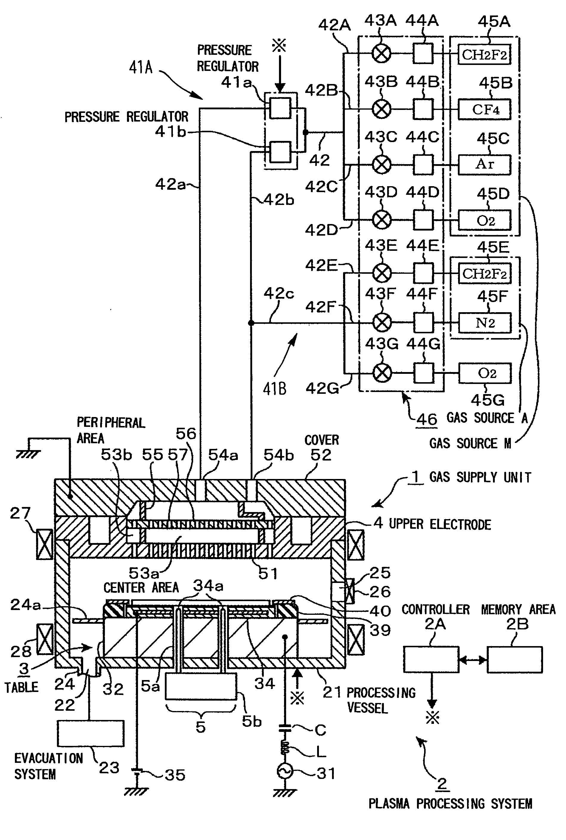
[0101] Prior to carrying out simulations, an experiment for estimating the amount of a gas to be generated from the wafer W in the step of etching the SiN film 74 was carried in order to determine more practical conditions. The SiN film 74 was etched under the following process conditions.

(Etching of Sin Film 74)

[0102] Frequency of high-frequency wave: 13.56 MHz

[0103] Power of high-frequency wave: 700 W

[0104] Process pressure: 18.7 Pa (140 mTorr)

[0105] Process gases (gas source M): [0106] CH2F2 / CF4 / Ar / O2=15 / 80 / 150 / 21 sccm

[0107] Process gas (gas source A): CH2F2=5 sccm

[0108] Pressures of pressure regulators: [0109] pressure regulator 41a / pressure regulator 41b=[0110] 55 / 45 (distance L=90 mm), [0111] 1 / 1 (distance L=110 mm), and [0112] 45 / 55 (distance L=130 mm)

Results of Experiments

[0113] The etching rates of the SiN film 74 determined in the above experiments are shown in Table 1.

TABLE 1Distance L (mm)90110130Etching Rate180.4181.3180.9(nm)Standard1.81.41.9D...

experimental example 2

Simulation

[0115] The gas distribution in the processing vessel 21 was simulated with the use of a fluid analysis soft, Fluent Vers. 6.2.16, manufactured by FLUENT Corp. The simulation was carried out on the assumption that gases are compressive fluids and that their flows are laminar. Further, calculations were made on the assumption that a gas causes slips in velocity and jumps in temperature on a solid surface such as a wafer W or upper electrode 4 surface.

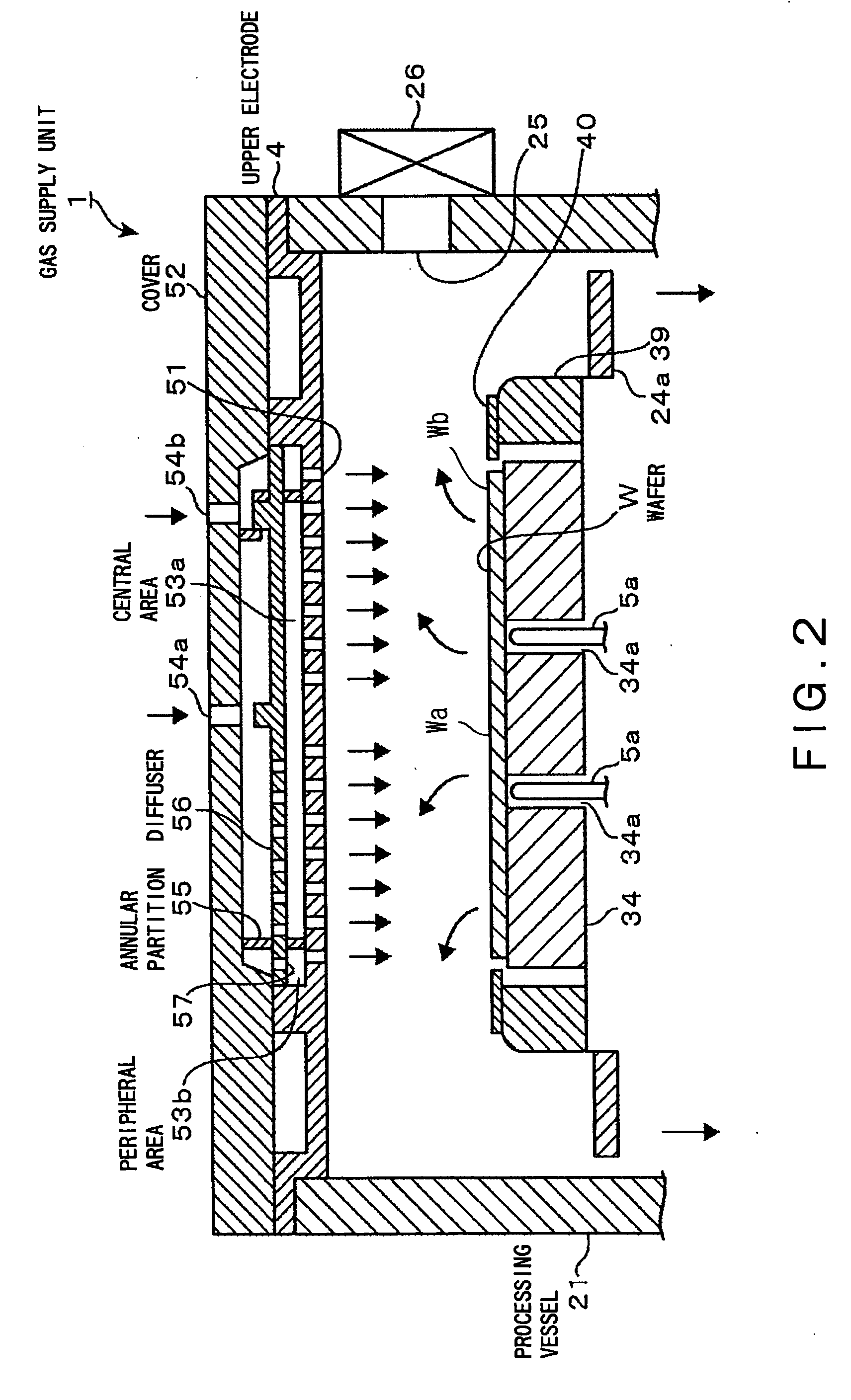
[0116] The distance L from the center of the upper electrode 4 to the partition 55 was, as shown in FIG. 5, made 90 mm, 110 mm, or 130 mm so that the radius of the outermost circle of the gas-jetting pores 51 communicating with the center section 53a was 53%, 67%, or 80% of the radius of the wafer W, respectively.

[0117] The simulations were carried out under the same process conditions as in the above-described Experimental Example 1, except that the process pressure was set to the following three levels and that the gas flow...

experimental example 3

Verification of Simulations

[0130] Experiments were carried out in order to verify the results of the simulations carried out in Experimental Example 2. In the experiments, the same processing process as in Experimental Example 1 was carried out, and the wafer W in the state as shown in FIG. 4(b) was etched. The process conditions used were the same as in Experimental Example 2, except for the following conditions.

(Process Conditions)

[0131] Distance L from the center of the upper electrode 4[0132] to the partition 55: as described above

[0133] Process pressure: 18.7 Pa (140 mTorr)

[0134] Process gases (gas source M): as described above

[0135] Process gas (gas source A): as described above


PUM

PropertyMeasurementUnit
pressureaaaaaaaaaa
sizeaaaaaaaaaa
temperatureaaaaaaaaaa

Abstract

The present invention is to provide a technique for uniformly processing a substrate surface in the process of processing a substrate by supplying a gas. The inside of a shower head having gas-jetting pores for supplying a gas to a substrate is partitioned into a center section from which a gas is supplied to the center portion of a substrate, and a peripheral section from which a gas is supplied to the peripheral portion of the substrate, and the same process gas is supplied to the substrate from these two sections at flow rates separately regulated. The distance from the center of the center section of the gas supply unit to the outermost gas-jetting pores in the center section is set 53% or more of the radius of the substrate. Moreover, an additional gas is further supplied to the peripheral portion of the substrate.

Description

CROSS-REFERENCE TO RELATED APPLICATIONS [0001] The present application for patent enjoys the benefit of the right to Japanese Patent Application No. 2006-221675 filed on Aug. 15, 2006 and U.S. Patent Provisional Application No. 60 / 875,538 filed on Dec. 19, 2006. The whole description in the aforesaid applications is incorporated herein by.reference.BACKGROUND OF THE INVENTION [0002] 1. Field of the Invention [0003] The present invention relates to a technique for processing a substrate, such as a semiconductor wafer, by supplying gases to it, and to a unit for supplying the gases. [0004] 2. Background Art [0005] In semiconductor device production processes, processing of a substrate such as a semiconductor wafer (hereinafter referred to as a wafer), e.g., etching or CVD, is conducted by placing a substrate in a processing vessel, and injecting, onto the substrate, process gases from a gas supply unit called a gas shower head, set in parallel with the substrate. [0006] On the other h...

Claims


Application Information

Patent Timeline
Patent Type & Authority Applications(United States)
IPC IPC(8): H01L21/306C23F1/00
CPCH01J37/3244H01L21/3086H01L21/31116H01J37/32449
Inventor MASUDA, NORIIKI
Owner TOKYO ELECTRON LTD
Why Eureka
Try Eureka