

Transistor And Method For Manufacturing The Same
- Summary
- Abstract
- Description
- Claims
- Application Information
AI Technical Summary
Benefits of technology
Problems solved by technology
Method used
Image

Examples
first embodiment
[0052]FIGS. 8A to 8C are diagrams for a method for manufacturing a transistor, wherein an end portion of a gate line is engaged with a trench of the valley structure in accordance with the invention.
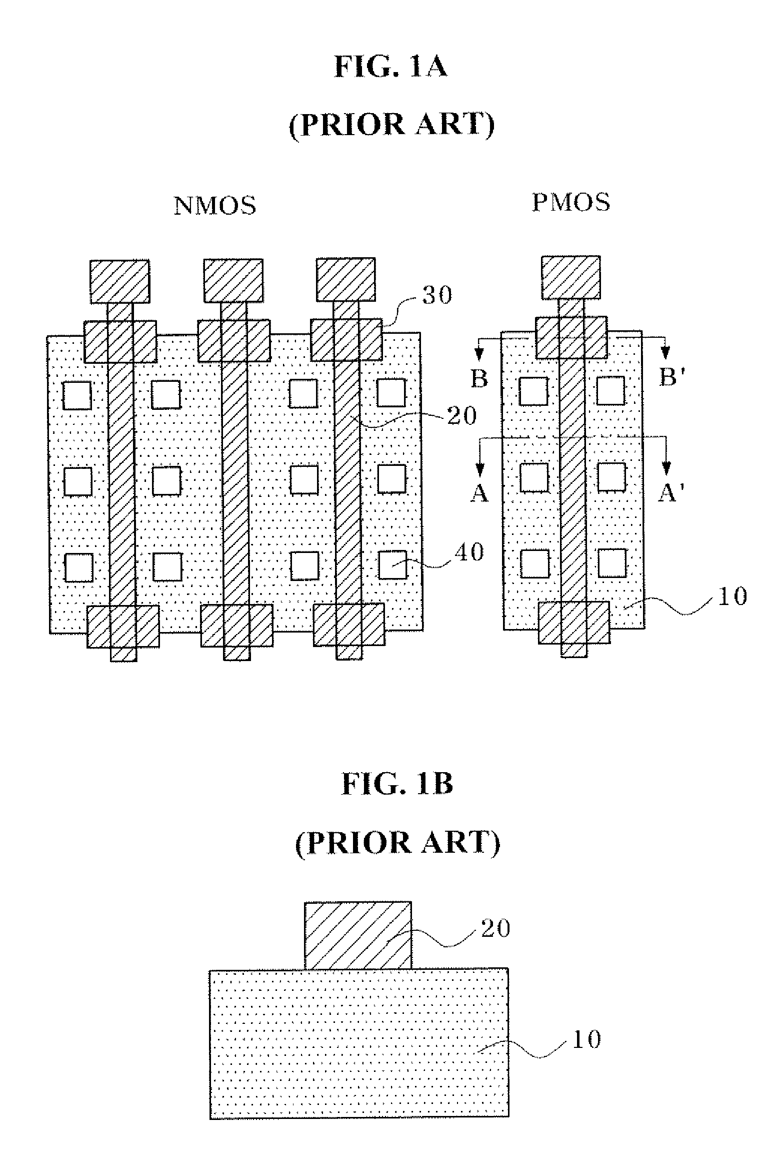
[0053]Referring to FIG. 5A, a photoresist film pattern 302 is formed on a semiconductor substrate 300 including a device isolation region to cover the substrate 300 in the cell region and selectively expose the substrate 300 in the peripheral circuit region. In the peripheral circuit region, it is preferable to expose only a region adjacent to the device isolation region to be engaged with the end portion of the gate line.
[0054]Referring to FIG. 8B, in the peripheral circuit region, the exposed region to be engaged with the end portion of the gate line is etched through a mask of the photoresist film pattern 302, so that a trench 304 of the valley structure is formed. The trench 304 of the valley structure may be formed in a rectangular shape.
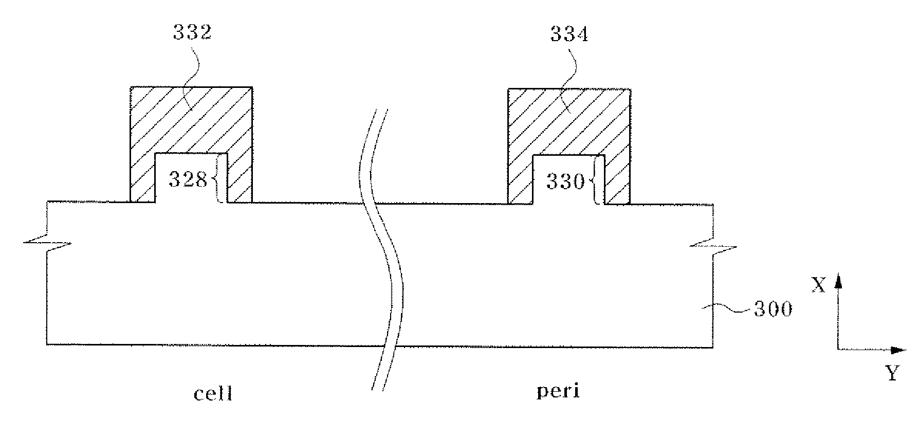
[0055]Then, as shown in FIG. 8C, gate lines 3...
second embodiment
[0056]FIGS. 9A to 9C are diagrams for a method for manufacturing a transistor, wherein an end portion of a gate line is engaged with a trench of the valley structure in accordance with the invention.
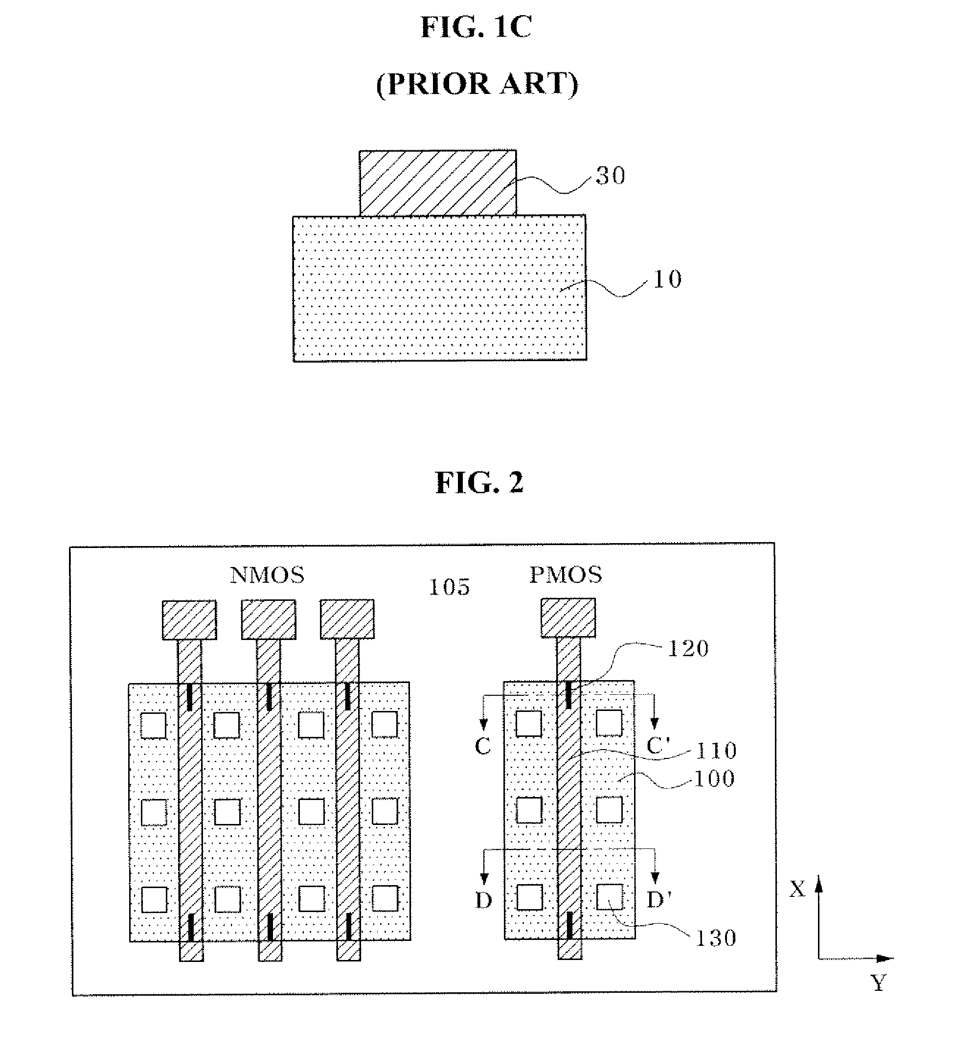
[0057]Referring to FIG. 9A, a photoresist film pattern 310 is formed on the semiconductor substrate 300 including the device isolation region to selectively expose the substrate 300 in the cell region and the peripheral circuit region. In this case, exposed regions in the cell region and the peripheral circuit region are regions for forming a recessed channel trench and a trench, respectively. In the peripheral circuit region, it is preferable to expose only an active region of the semiconductor substrate 300 to be engaged with the end portion of the gate line, adjacent to the device isolation region.
[0058]Referring to FIG. 9B, the exposed regions in the cell region and the peripheral circuit region are etched through a mask of the photoresist film pattern 310, so that trenches 311 and 3...
third embodiment
[0061]FIGS. 10A to 10C are diagrams for a method for manufacturing a transistor, wherein an end portion of a gate line engages a protrusion of the mesa structure in accordance with the invention.
[0062]Referring to FIG. 10A, a photoresist film pattern 318 is formed on the semiconductor substrate 300 including the device isolation region to cover the substrate 300 in the cell region and selectively cover the substrate 300 in the peripheral circuit region. In the peripheral circuit region, it is preferable to cover only an active region of the semiconductor substrate 300 adjacent to the device isolation region to be engaged with the end portion of the gate line.
[0063]Referring to FIG. 10B, in the peripheral circuit region, an exposed region in the peripheral circuit region is etched through a mask of the photoresist film pattern 318, so that a protrusion 320 of the mesa structure having a flat top surface is formed to be protruded from the surface of the substrate. The protrusion 320 o...
PUM
 Abstract
Description
Claims
Application Information