Plasma display panel and method of manufacturing the same

a technology of plasma display panel and display plate, which is applied in the manufacture of electrode systems, cold cathode manufacturing, and electric discharge tube/lamp manufacture, etc., can solve the problems of strength, uneven shape, cracking of ribs, and ribs falling, so as to improve the light emission efficiency of plasma display panel, increase the height of ribs, and increase the discharge space

a technology of plasma display panel and display plate, which is applied in the manufacture of electrode systems, cold cathode manufacturing, and electric discharge tube/lamp manufacture, etc., can solve the problems of strength, uneven shape, cracking of ribs, and ribs falling, so as to improve the light emission efficiency of plasma display panel, increase the height of ribs, and increase the discharge space

US20080079363A1Inactive Publication Date: 2008-04-03FUJITSU HITACHI PLASMA DISPLAY LTD

Image

  • Plasma display panel and method of manufacturing the same
  • Plasma display panel and method of manufacturing the same
  • Plasma display panel and method of manufacturing the same

Examples


Embodiment Construction

[0019]An embodiment of the present invention will be described below with reference to the drawings.

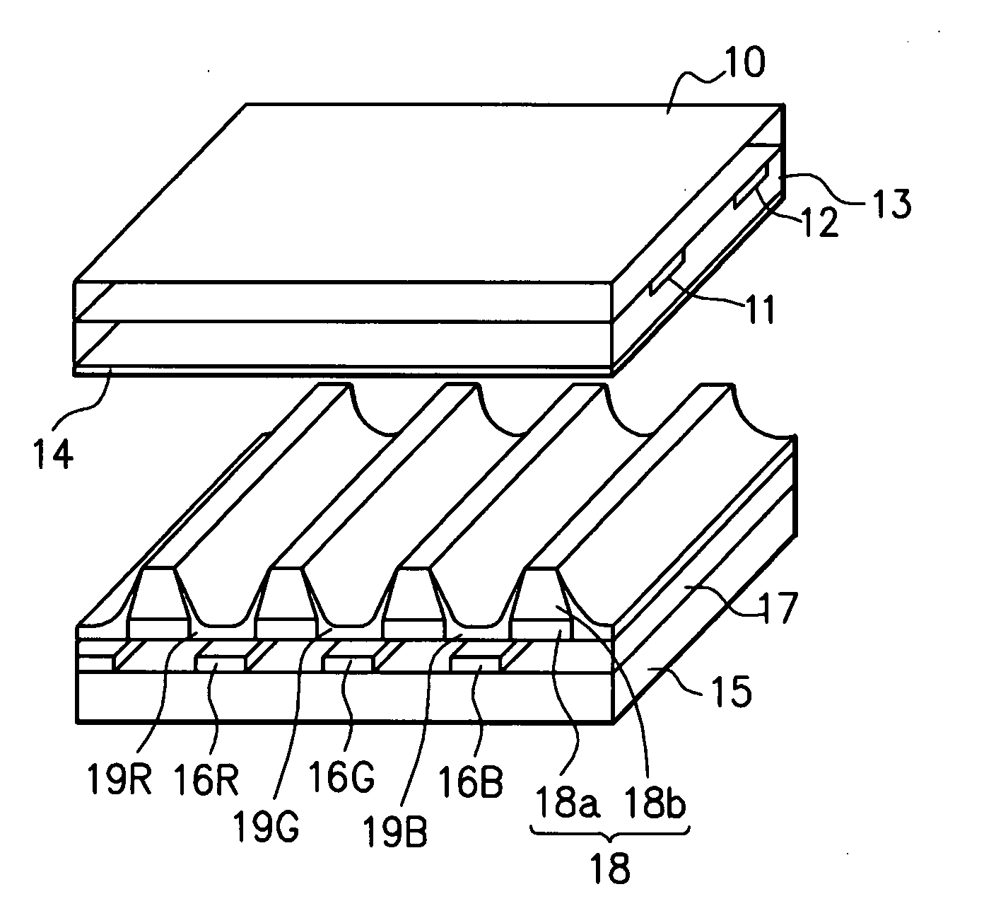
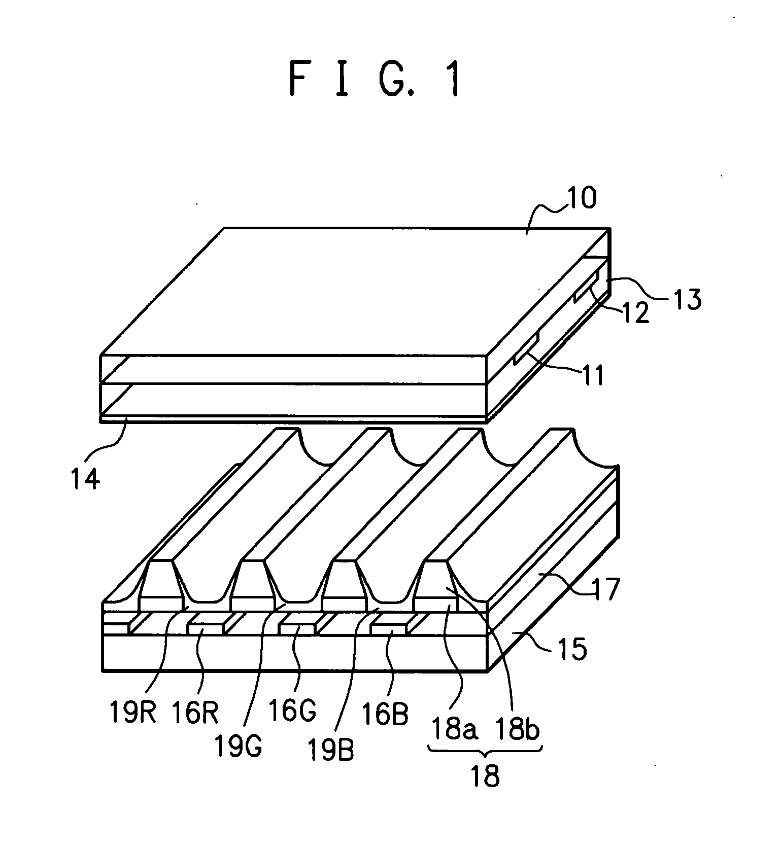
[0020]FIG. 1 is an exploded perspective view showing a configuration example of a plasma display panel in an embodiment of the present invention.

[0021]On a front glass substrate 10, X electrodes (sustain electrodes) 11 and Y electrodes (scanning electrodes) 12 that perform sustain discharge are formed arranged in parallel and alternately. On the electrodes 11 and 12, a dielectric layer 13 made of low-melting glass or the like is deposited. On the dielectric layer 13, an MgO (magnesium oxide) protective layer 14 is further deposited. In other words, the X electrodes 11 and the Y electrodes 12 arranged on the front glass substrate 10 are covered by the dielectric layer 13 whose surface is further covered by the protective layer 14.

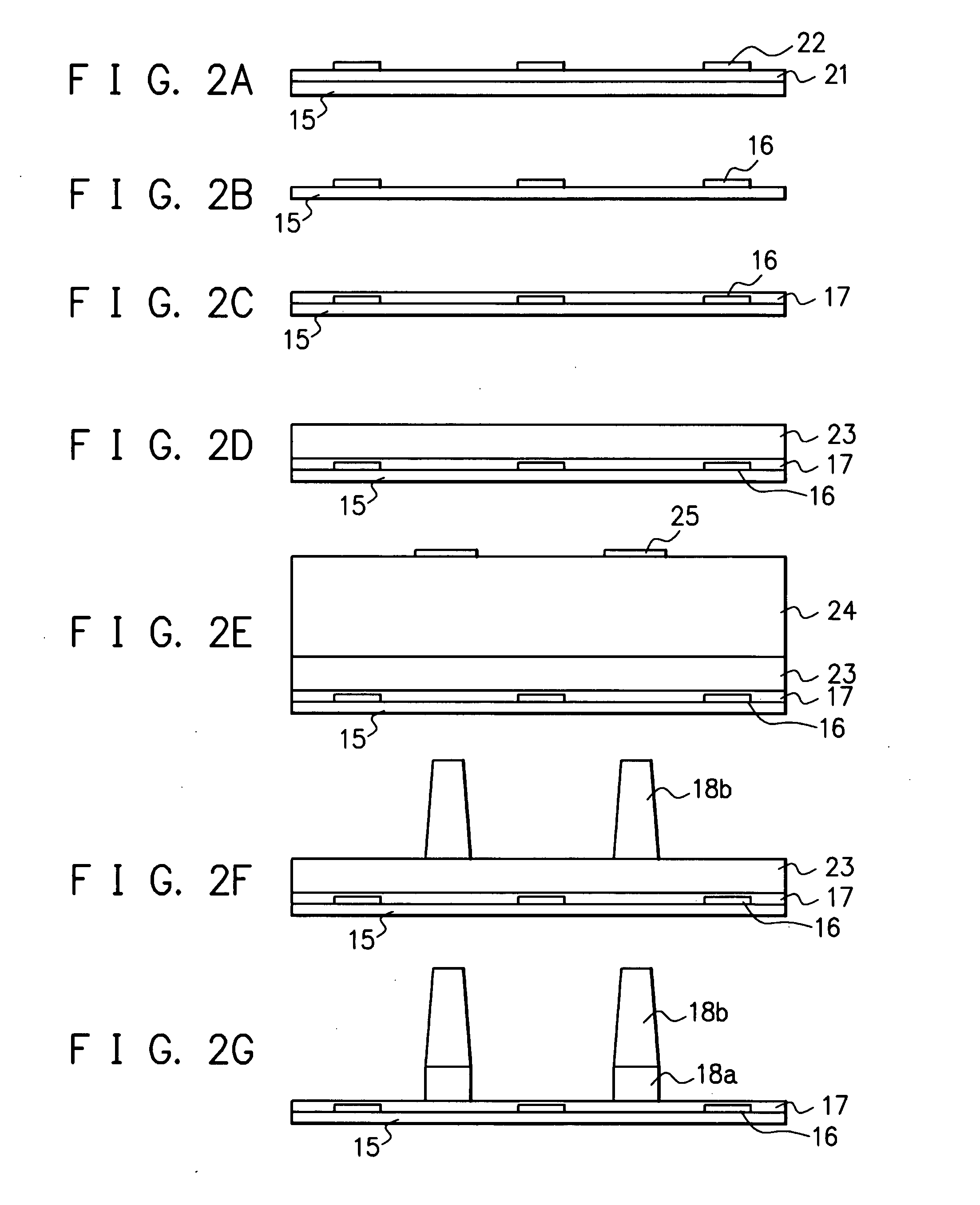
[0022]Besides, on a rear glass substrate 15 arranged opposed to the front glass substrate 10, address electrodes 16R, 16G, and 16B are formed in a direction p...


PUM


Abstract

In a plasma display panel having a discharge gas sealed in a gap between a front side substrate and a rear side substrate opposed to each other and having ribs partitioning a gas-sealed space into a discharge cell array arranged above an inner surface of one of the substrates, the rib includes an upper-layer rib and a lower-layer rib, and the upper-layer rib and the lower-layer rib are made of rib materials different from each other in resistance to etching, thereby allowing for formation of high ribs to enlarge the discharge space without affecting the upper-layer ribs when forming the lower-layer ribs.

Description

CROSS-REFERENCE TO RELATED APPLICATIONS[0001]This application is based upon and claims the benefit of priority from the prior Japanese Patent Application No. 2006-268877, filed on Sep. 29, 2006, the entire contents of which are incorporated herein by reference.BACKGROUND OF THE INVENTION[0002]1. Field of the Invention[0003]The present invention relates to a plasma display panel and a method of manufacturing the same.[0004]2. Description of the Related Art[0005]As a flat-type display device, a plasma display device with a plasma display panel (PDP) is put into practical use in which pixels on the screen are caused to emit light according to display data. In a plasma display panel of a surface discharge type, a plurality of surface discharge electrodes are formed on the inner surface of the front glass substrate, and the surface discharge electrodes are covered by a dielectric layer and a protective layer. On the inner surface of the rear glass substrate, ribs are formed, and phosphor...

Claims


Application Information

Patent Timeline
03 Apr 2008
Publication
US20080079363A1
IPC
H01J11/02; H01J9/02; H01J11/22; H01J11/24; H01J11/34; H01J11/36; H01J11/38
CPC
H01J11/12; H01J2211/366; H01J11/36; H01J11/38
Inventors
YOSHINAGA, TAKASHI; KAWASAKI, TATSUHIKO