Liquid crystal display device

a display device and liquid crystal technology, applied in the field of liquid crystal display devices, can solve the problems of user manipulation, troublesome manipulation, difficult to see images displayed in dark places, etc., and achieve the effect of preventing the degradation of ambient light photosensor elements

Inactive Publication Date: 2008-04-03
JAPAN DISPLAY WEST
View PDF15 Cites 48 Cited by
  • Summary
  • Abstract
  • Description
  • Claims
  • Application Information

AI Technical Summary

Benefits of technology

[0013] An advantage of some aspect of the invention is to provide a liquid crystal display device utilizing a thin film transistor (TFT) as an ambient light photosensor, and preventing the degradation of an ambient light photosensor element due to a biased polarity voltage applied to the TFT's gate electrode.
[0014] Another advantage of some aspect of the invention is to provide a liquid crystal display device preventing the breakage of a control circuit element coupled to the device's ambient light photosensor by means of a device for preventing the degradation of an ambient light photosensor element.
[0015] Further another advantage of some aspect of the invention is to provide a liquid crystal display device having a less power-consuming photodetector unit including an ambient light photosensor.

Problems solved by technology

In such liquid crystal display devices, liquid crystals are non light-emitting, which means that images displayed are hard to see in dark places.
However, manual on / off controlling of such backlight requires the user's manipulation according to the brightness of external light.
Such manipulations are bothersome, and the user sometimes ends up turning the backlight on even in bright places.
In this case, using such display in a mobile telephone or similar equipment could cause the battery to run down quickly.
This results in charge being trapped on the TFT gate electrode, thereby causing degradation or characteristic change in a TFT sensor element, and reduced sensitivity of the sensor.
As a result, a precise photodetection cannot be performed.
However, when applying such reset signal to the photodetector circuit, it is difficult to control the applying timing.
Therefore, for example, when applying such signal during charging or reading to / from the ambient light photosensor, there is a risk of causing the photodetector unit and the reader to malfunction.
Also, when applying at other timing, a sequence control of controlling resetting, charging, and reading becomes necessary, therefore making the control circuit configuration complicated.
Accordingly, there is a risk of damaging the external circuit element coupled to the output line.
Accordingly, excess power consumption increases which causes quick battery drain.

Method used


Image

  • Liquid crystal display device
  • Liquid crystal display device
  • Liquid crystal display device

Examples


first embodiment

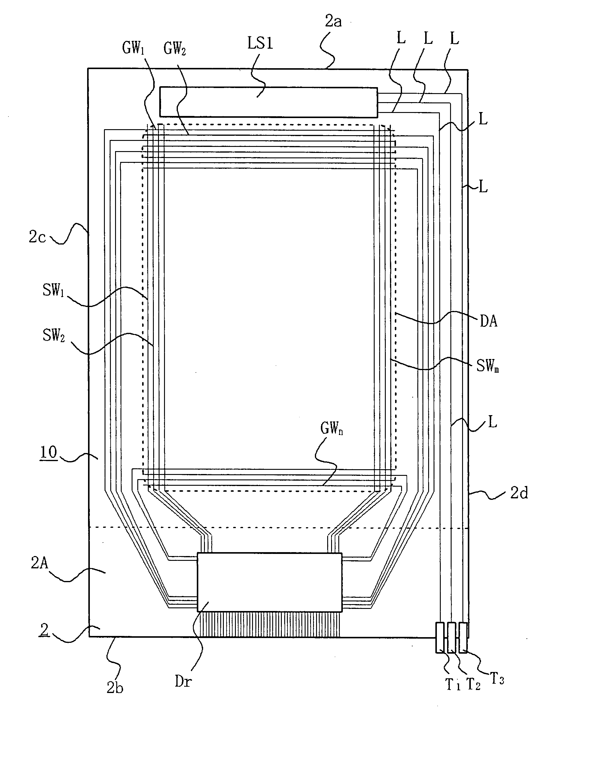
[0047]FIG. 1 is a plan view schematically showing an active matrix substrate seen through a color filter substrate included in a liquid crystal display device according to a first embodiment of the invention.

[0048] As shown in FIG. 1, the liquid crystal display device 1 includes an active matrix substrate (“TFT substrate” below) 2 and a color filter substrate (“CF substrate” below”) 10 having various wiring lines formed on, for example, a rectangular transparent material such as glass and deployed opposing each other. The TFT substrate 2 is of a larger size than the CF substrate 10, so that when it is positioned opposing the CF substrate 10, an overhang portion 2A of a particular extent is formed. The structure is such that a seal material (not shown) is stuck around the peripheries of the TFT substrate 2 and the CF substrate 10, and a liquid crystal and spacers are sealed into the interior space therebetween.

[0049] On the opposed faces of the TFT substrate 2 and CF substrate 10, ...

second embodiment

[0074] Referring to FIG. 7 and FIG. 8, a liquid crystal display device according to the second embodiment of the invention will now be described. FIG. 7 is an equivalent circuit diagram of a photodetector unit built in a liquid crystal display device according to a second embodiment of the present invention. FIG. 8 is an operational waveform chart of a controller of FIG. 7.

[0075] The liquid crystal device is the same as that of the first embodiment except that a part of the photodetector unit differs. The description other than the photodetector unit will be omitted with the aid of the description of the first embodiment.

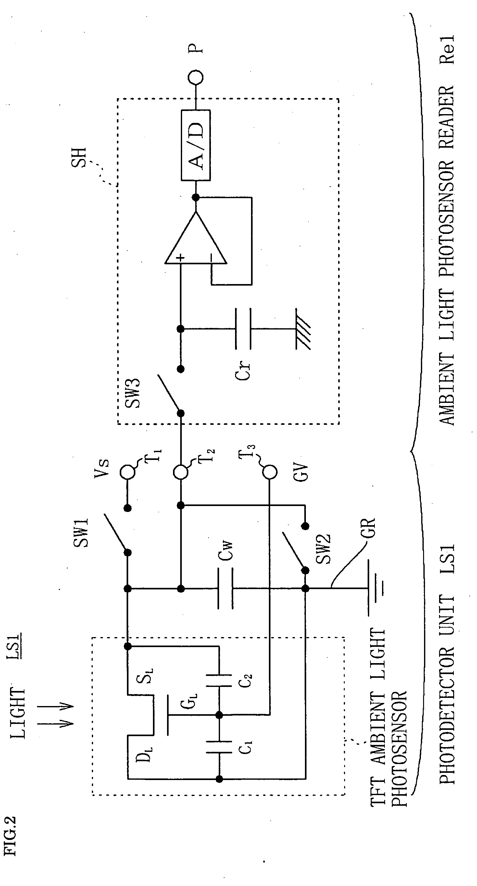
[0076] A photodetector unit LS2 has a structure in which a resistor Rg is coupled to a gate line coupled to the gate electrode GL other than the switching element SW2 of the photodetector unit LS1 of the embodiment 1. And further, this gate line is grounded GR via a capacitor Cg.

[0077] When applying a gate voltage GV of a rectangular wave in a state where the res...


PUM

PropertyMeasurementUnit
reverse bias voltage GVaaaaaaaaaa
constant standard voltageaaaaaaaaaa
reverse bias voltageaaaaaaaaaa

Abstract

A liquid crystal display device 1 according to an embodiment of the present invention includes a liquid crystal display panel, a photodetector unit LS1 that is built into the liquid crystal display panel and has a TFT ambient light photosensor, an ambient light photosensor reader Re1 for reading a voltage due to photo-leakage from the TFT ambient light photosensor, and a control means 20 for controlling the photodetector unit and the ambient light photosensor reader, and a backlight 24, etc., according to an output from the ambient light photosensor reader. The photodetector unit has a switching element SW2 coupled between a source line coupled to the TFT ambient light photosensor's source electrode SL and a drain line coupled to the TFT ambient light photosensor's drain electrode DL. The control means 20 makes the source line and the drain line of the TFT ambient light photosensor be coupled to a common potential when changing a gate voltage of the TFT ambient light photosensor by keeping the switching element SW2 turned on. It is therefore possible to provide a liquid crystal display device that utilizes a thin film transistor as an ambient light photosensor and prevents degradation of an ambient light photosensor element due to a biased polarity voltage applied to the gate electrode.

Description

BACKGROUND [0001] 1. Technical Field [0002] The present invention relates to a liquid crystal display device having an illuminating unit for illuminating a liquid crystal display panel, and more particularly to a liquid crystal display device in which an ambient light photosensor that senses external light is built into the liquid crystal display panel, and which the device controls the illuminating unit according to an output from such ambient light photosensor. [0003] 2. Related Art [0004] Over recent years, particularly, liquid crystal display devices have been widely used not only in information and telecommunications equipment but also in electrical equipment in general. In such liquid crystal display devices, liquid crystals are non light-emitting, which means that images displayed are hard to see in dark places. Therefore these devices are provided with a backlight or a sidelight, etc., and when the external light is dim, such backlight is lit in order to illuminate the image...

Claims


Application Information

Patent Timeline
Patent Type & Authority Applications(United States)
IPC IPC(8): G02F1/13357G02F1/1368
CPCG02F1/13318G02F1/1362G02F2001/133626G09G2330/022G09G3/3611G09G2300/043G09G2320/0219G09G3/3406G02F1/133626G02F1/133
Inventor KUNIMORI, TAKASHISANO, YUTAKAYASUMORI, MASANORI
Owner JAPAN DISPLAY WEST
Why Eureka
Try Eureka