Deposition and densification process for titanium nitride barrier layers

a technology of titanium nitride and densification process, which is applied in the direction of semiconductor/solid-state device manufacturing, basic electric elements, electric devices, etc., can solve the problems of large amount of ongoing effort, failure of device, and difficulty in deposition process

Inactive Publication Date: 2008-04-10
APPLIED MATERIALS INC
View PDF99 Cites 52 Cited by
  • Summary
  • Abstract
  • Description
  • Claims
  • Application Information

AI Technical Summary

Benefits of technology

[0012]In one embodiment, a method for forming a titanium nitride barrier material on a substrate is provided which includes depositing a first titanium nitride layer on the substrate by a thermal metal-organic chemical vapor deposition (MOCVD) process, and thereafter, densifying the first titanium nitride layer by exposing the substrate to a plasma process. In one example, the method provides forming a titanium nitride barrier stack by depositing a second titanium nitride layer on the first titanium nitride layer by the thermal MOCVD process and densifying the second titanium nitride layer by exposing the substrate to the plasma process. In another example, the method provides forming a titanium nitride barrier stack by depositing a third titanium nitride layer on the second titanium nitride layer by the thermal MOCVD process and densifying the third titanium nitride layer by exposing the substrate to the plasma process. Therefore, the titanium nitride barrier material may contain a single densified titanium nitride layer or a titanium nitride barrier stack containing two, three, or more densified titanium nitride layers. Subsequently, the method provides depositing a conductive material on the substrate and exposing the substrate to a thermal annealing process.

Problems solved by technology

However, as the fringes of circuit technology are pressed, the shrinking dimensions of interconnects in VLSI and ULSI technology have placed additional demands on the processing capabilities.
Many traditional deposition processes have difficulty filling submicron structures where the aspect ratio exceeds 4:1.
Therefore, there is a great amount of ongoing effort being directed at the formation of substantially void-free and seam-free submicron features having high aspect ratios.
A variety of problems that eventually may lead to device failure is a result from the specific process used to deposit or form the titanium nitride layer.
Reliability problems may occur from the use of titanium tetrachloride as a chemical precursor to form a titanium nitride layer during a CVD process.
In particular, the titanium nitride layer may have poor adhesion over the titanium layer, resulting in peeling of the titanium nitride layer from the titanium layer.
Another problem arises since the titanium tetrachloride precursor produces chlorine which diffuses and contaminates neighboring materials (e.g., dielectric or conductive) on the substrate.
Often, this diffusion problem occurs because the barrier layer is too thin or contains a barrier material not dense enough (e.g., too porous) to prohibit or limit the diffusing metallic atoms.
However, the resistance of a barrier layer increases proportional to the thickness, as does the time and cost for deposition.

Method used


Image

  • Deposition and densification process for titanium nitride barrier layers
  • Deposition and densification process for titanium nitride barrier layers
  • Deposition and densification process for titanium nitride barrier layers

Examples


examples

200 mm TXZ® Chamber

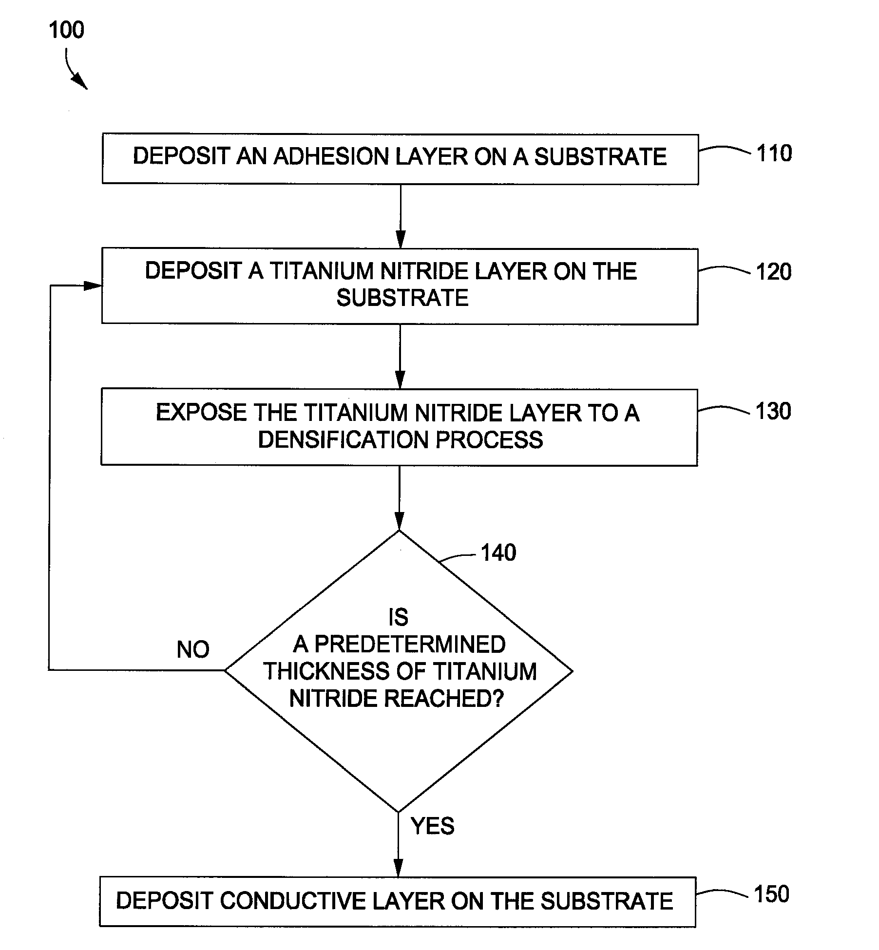
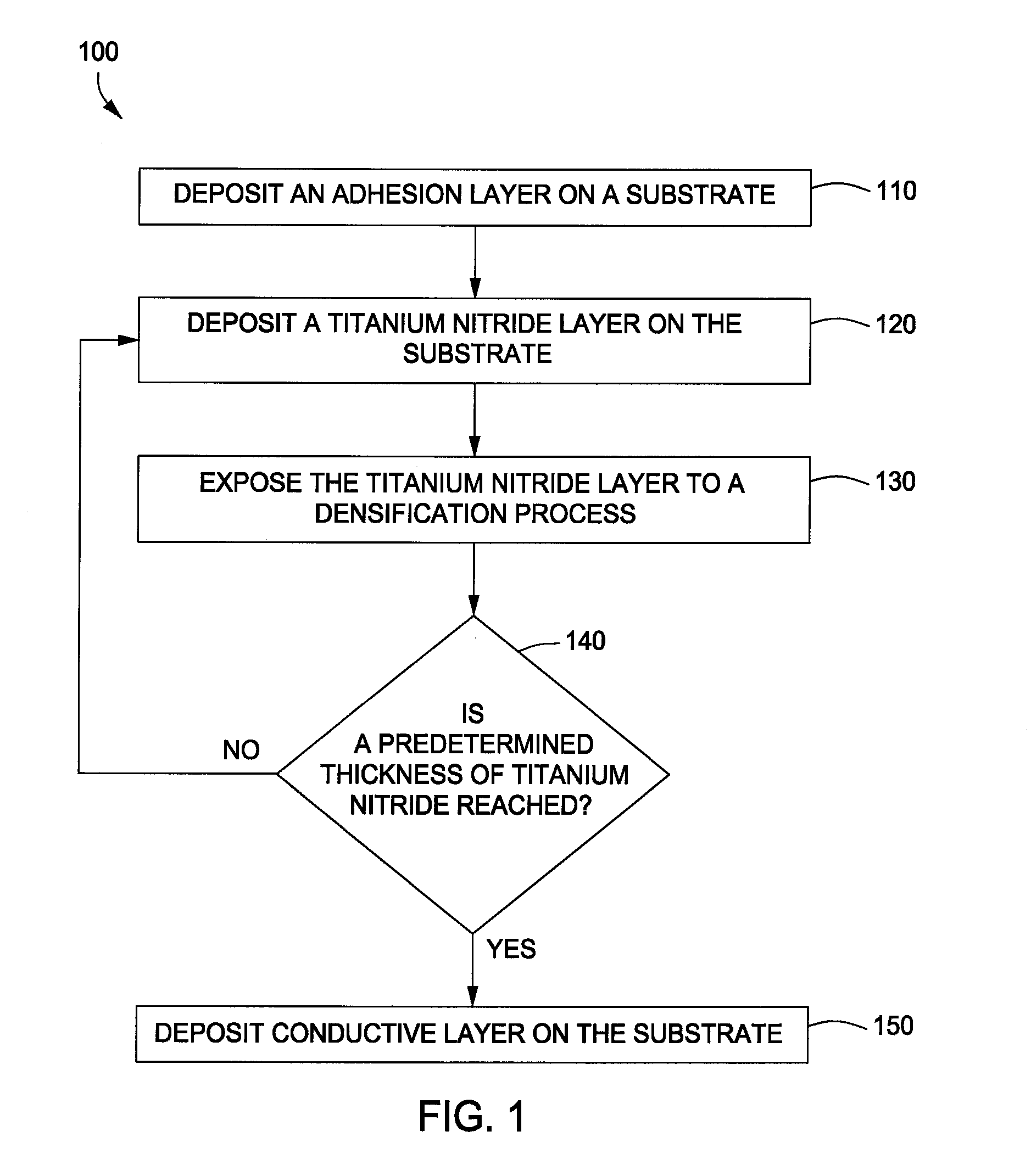
[0053]A high-pressure process in a TXZ® chamber, available from Applied Materials, Inc., located in Santa Clara, Calif., is used for formation of the titanium nitride barrier layer. Low-resistivity titanium nitride thin-films are thermally deposited using a high-pressure MOCVD process. The chamber is plumbed to a titanium precursor, such as TDMAT or TDEAT. The titanium nitride thin film is subsequently plasma post treated with a hydrogen-nitrogen plasma generated by a high plasma power within a range from about 750 watts to about 1,250 watts in order to reduce the film resistivity.

Overview of the Formation of Titanium Nitride Barrier Layer

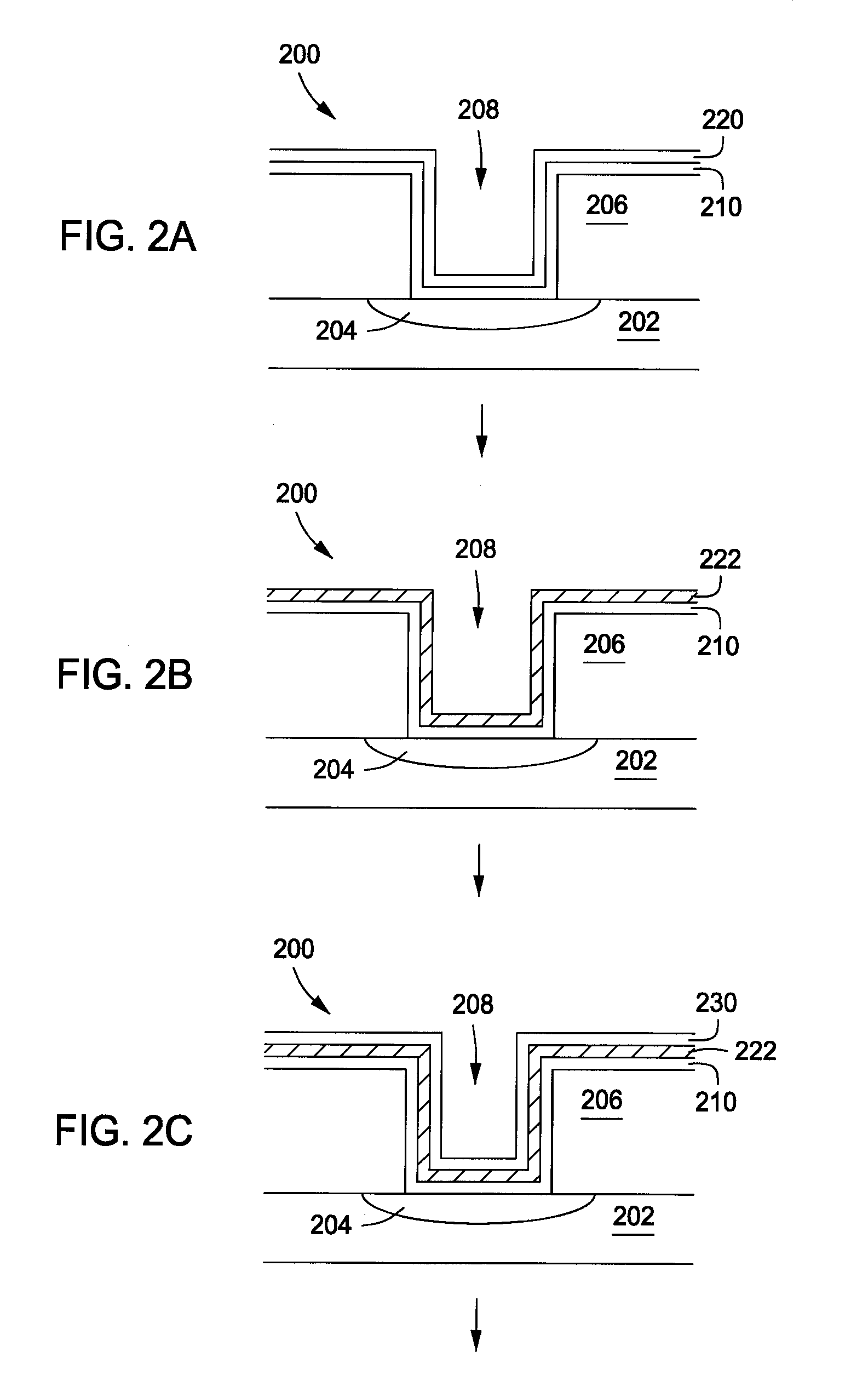
[0054]The substrate is heated to a predetermined temperature (e.g., about 360° C.). TDMAT is vaporized and exposed to the substrate to thermally decompose as a film deposited on the substrate surface at a low temperature of about 360° C. which corresponds to a heater temperature of about 380° C. and at a high chamber pressure of ...


PUM

PropertyMeasurementUnit
timeaaaaaaaaaa
temperatureaaaaaaaaaa
thicknessaaaaaaaaaa

Abstract

In one embodiment, a method for forming a titanium nitride barrier material on a substrate is provided which includes depositing a titanium nitride layer on the substrate by a metal-organic chemical vapor deposition (MOCVD) process, and thereafter, densifying the titanium nitride layer by exposing the substrate to a plasma process. In one example, the MOCVD process and the densifying plasma process is repeated to form a barrier stack by depositing a second titanium nitride layer on the first titanium nitride layer. In another example, a third titanium nitride layer is deposited on the second titanium nitride layer. Subsequently, the method provides depositing a conductive material on the substrate and exposing the substrate to a annealing process. In one example, each titanium nitride layer may have a thickness of about 15 Å and the titanium nitride barrier stack may have a copper diffusion potential of less than about 5×10¹⁰ atoms/cm2.

Description

CROSS-REFERENCE TO RELATED APPLICATION[0001]This application claims benefit of U.S. Ser. No. 60 / 828,739 (APPM / 011097L), filed Oct. 9, 2006, which is herein incorporated by reference in its entirety.BACKGROUND OF THE INVENTION[0002]1. Field of the Invention[0003]Embodiments of the invention generally relate to a fabrication process for depositing a barrier layer on a substrate, and more particularly to a deposition and densification process for forming a titanium nitride barrier material.[0004]2. Description of the Related Art[0005]Reliably producing submicron and smaller features is one of the key technologies for the next generation of very large scale integration (VLSI) and ultra large scale integration (ULSI) of semiconductor devices. However, as the fringes of circuit technology are pressed, the shrinking dimensions of interconnects in VLSI and ULSI technology have placed additional demands on the processing capabilities. The multilevel interconnects that lie at the heart of thi...

Claims


Application Information

Patent Timeline
Patent Type & Authority Applications(United States)
IPC IPC(8): H01L21/31
CPCH01L21/28556H01L21/76862H01L21/76843H01L21/321
Inventor KHANDELWAL, AMITGELATOS, AVGERINOS V.MARCADAL, CHRISTOPHECHANG, MEI
Owner APPLIED MATERIALS INC
Why Eureka
Try Eureka