Nitride Semiconductor Light Emitting Device And Fabrication Method Thereof

a light emitting device and semiconductor technology, applied in the direction of semiconductor/solid-state device manufacturing, semiconductor devices, semiconductor devices, etc., can solve the problems of improving the optical output and achieve the effect of improving the crystal property of the activation layer, improving the optical output and the reliability of the light emitting devi

Active Publication Date: 2008-04-17
SUZHOU LEKIN SEMICON CO LTD
View PDF8 Cites 4 Cited by
  • Summary
  • Abstract
  • Description
  • Claims
  • Application Information

AI Technical Summary

Benefits of technology

[0017] According to the nitride semiconductor light emitting device of the present invention and the method of manufacturing the same, it is possible to improve the crystal property of the activation layer that forms the nitride semiconductor light emitting device and to improve the optical output and the reliability of the light emitting device.

Problems solved by technology

Also, it has limitations on improving the optical output of the light emitting device during the growth of the crystal of the nitride semiconductor without improving the design of the light emitting device and the crystal properties of the emission layer and the p-GaN layer in order to improve internal quantum efficiency.

Method used


Image

  • Nitride Semiconductor Light Emitting Device And Fabrication Method Thereof
  • Nitride Semiconductor Light Emitting Device And Fabrication Method Thereof
  • Nitride Semiconductor Light Emitting Device And Fabrication Method Thereof

Examples


first embodiment

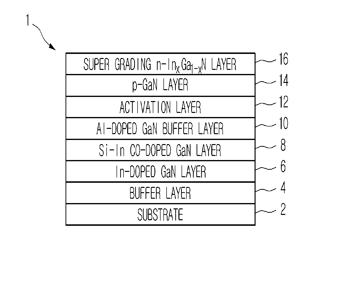
[0026]FIG. 1 schematically illustrates the stacked structure of a nitride semiconductor light emitting device according to the present invention.

[0027] As illustrated in FIG. 1, in the nitride semiconductor light emitting device 1 according to the present invention, a buffer layer 4 is formed on a substrate 2. Here, the buffer layer 4 may have a structure selected from the group consisting of an AlInN / GaN stacked structure, an InGaN / GaN super lattice structure, an InXGa1−XN / GaN stacked structure, and an AlXInYGa1−(X+Y)N / InXGa1−XN / GaN stacked structure (0≦x≦1, 0≦y≦1, x+y≦1).

[0028] An In-doped GaN layer 6 is formed on the buffer layer 4 and an n-type first electrode layer is formed on the In-doped GaN layer 6. Here, Si—In co-doped GaN layer 8 may be used as the n-type first electrode layer.

[0029] Also, an Al-doped GaN buffer layer 10 is formed on the Si—In co-doped GaN layer 8 and an activation layer 12 that emits light is formed on the Al-doped GaN buffer layer 10. The activation l...

second embodiment

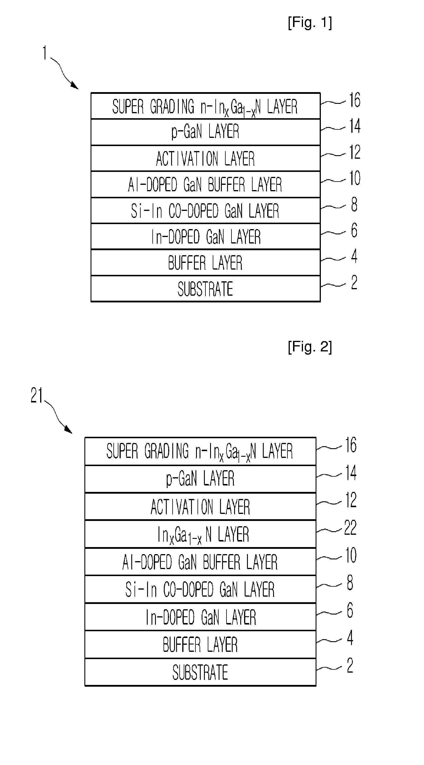
[0042] On the other hand, FIG. 2 schematically illustrates the stacked structure of a nitride semiconductor light emitting device according to the present invention. In the stacked structure illustrated in FIG. 2, description of the layer (denoted by the same reference numeral) described with reference to FIG. 1 will be omitted.

[0043] A nitride semiconductor light emitting device 21 according to the second embodiment of the present invention is different from the nitride semiconductor light emitting device 1 according to the first embodiment illustrated in FIG. 1 in that an InXGa1−XN layer 22 containing a small amount of Indium is further included.

[0044] That is, according to the nitride semiconductor light emitting device 21 according to the second embodiment of the present invention, the InXGa1−XN layer 22 containing a small amount of Indium is further formed between the Al-doped GaN buffer layer 10 and the activation layer 12. In order to improve internal quantum efficiency, the...

third embodiment

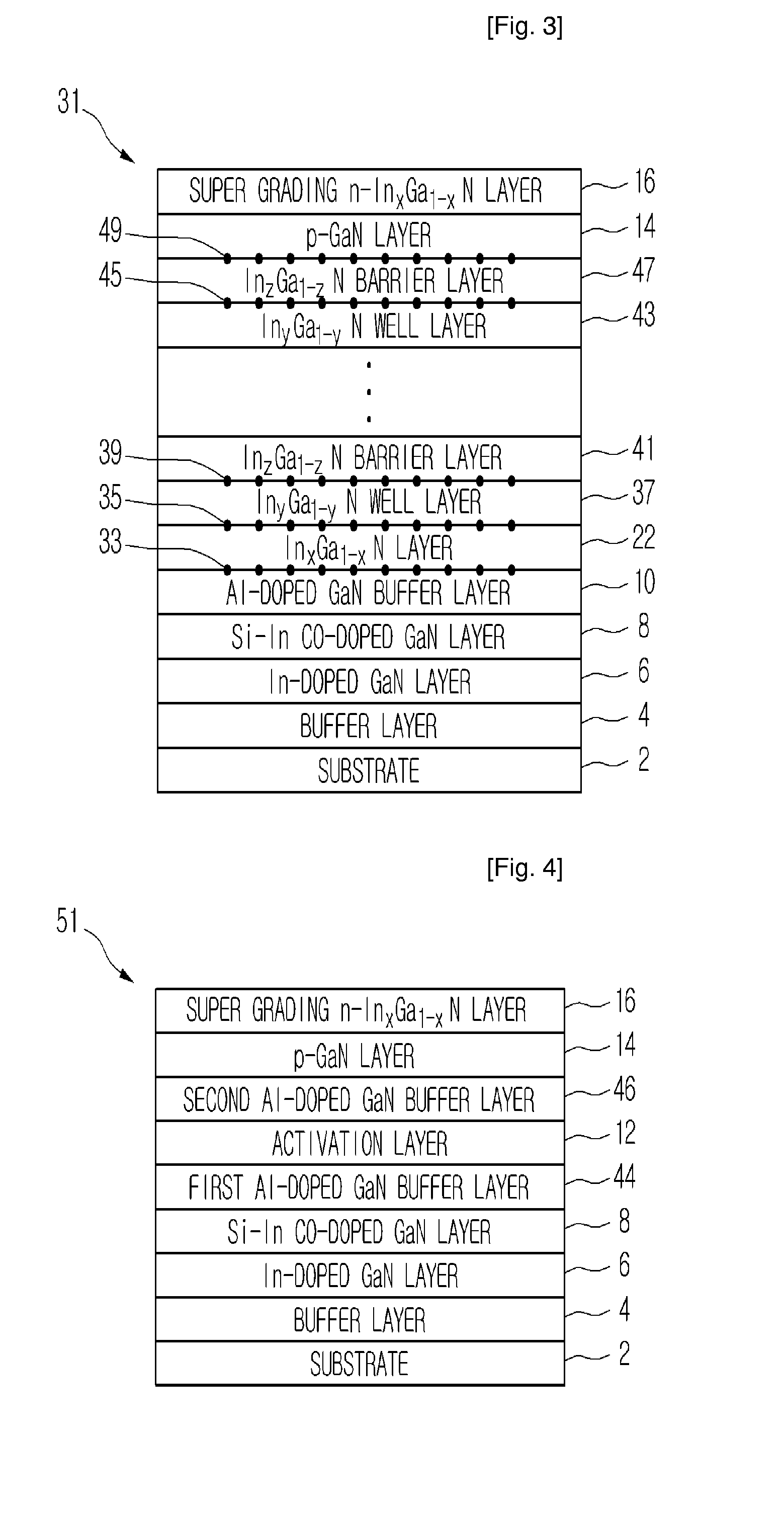
[0045] Then, the structure of the activation layer applied to a nitride semiconductor light emitting device 31 according to the present invention will be described in detail with reference to FIG. 3. FIG. 3 schematically illustrates the stacked structure of a nitride semiconductor light emitting device according to the present invention. In the stacked structure illustrated in FIG. 3, description of the layer (denoted by the same reference numeral) described with reference to FIG. 1 will be omitted.

[0046] In a nitride semiconductor light emitting device 31 according to the third embodiment of the present invention, as illustrated in FIG. 3, in order to increase the internal quantum efficiency, the low-mole InXGa1−XN layer 22 containing a small amount of Indium that controls the strain of the activation layer is formed. Also, in order to improve optical output and reverse leakage current caused by fluctuation in Indium, SiNX cluster layers 33 and 35 controlled in the form of an atomi...


PUM


Abstract

A nitride semiconductor light emitting device includes a first nitride semiconductor layer, a first Al-doped nitride semiconductor buffer layer formed on the first nitride semiconductor layer, an activation layer formed on the first Al-doped nitride semiconductor buffer layer, and a second nitride semiconductor layer formed on the activation layer. Another nitride semiconductor light emitting device includes a first nitride semiconductor layer, an activation layer formed on the first nitride semiconductor layer, a second Al-doped nitride semiconductor buffer layer formed on the activation layer, and a second nitride semiconductor layer formed on the second Al-doped nitride semiconductor buffer layer. Still another nitride semiconductor light emitting device includes a first nitride semiconductor layer, a first Al-doped nitride semiconductor buffer layer formed on the first nitride semiconductor layer, an activation layer formed on the first Al-doped nitride semiconductor buffer layer, a second Al-doped nitride semiconductor buffer layer formed on the activation layer, and a second nitride semiconductor layer formed on the second Al-doped nitride semiconductor buffer layer.

Description

TECHNICAL FIELD [0001] The present invention relates to a nitride semiconductor light emitting device and a method of manufacturing the same. BACKGROUND ART [0002] In general, GaN based nitride semiconductor is applied to electronic devices that are high speed switching and high output devices such as blue and green light emitting diodes (LED), metal semiconductor field effect transistors (MESFET), and high electron mobility transistors (HEMT). In particular, the blue and green LEDs have already been produced and the global sales of the blue and green LEDs have exponentially increased. [0003] The GaN based nitride semiconductor light emitting device is grown on a sapphire substrate or a SiC substrate. Then, an AlYGa1−YN polycrystalline thin film is grown on the sapphire substrate or the SiC substrate as a buffer layer at a low growth temperature. Then, an undoped GaN layer, a Si-doped n-GaN layer, or a mixture of the above two structures is grown on the buffer layer at a high temper...

Claims


Application Information

Patent Timeline
Patent Type & Authority Applications(United States)
IPC IPC(8): H01L33/00H01L21/02H01L29/06H01L33/06H01L33/12H01L33/32
CPCH01L33/007H01L33/025H01L33/32H01L33/26H01L33/12
Inventor LEE, SUK HUN
Owner SUZHOU LEKIN SEMICON CO LTD
Why Eureka
Try Eureka