

Display device having photosensor and method of fabricating the same
- Summary
- Abstract
- Description
- Claims
- Application Information
AI Technical Summary
Benefits of technology
Problems solved by technology
Method used
Image

Examples
first embodiment
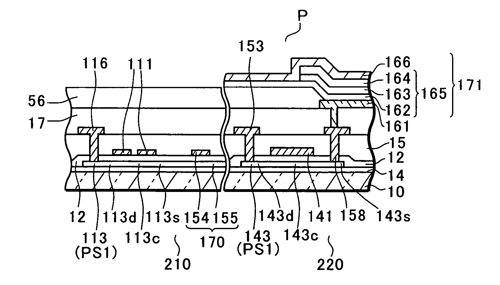
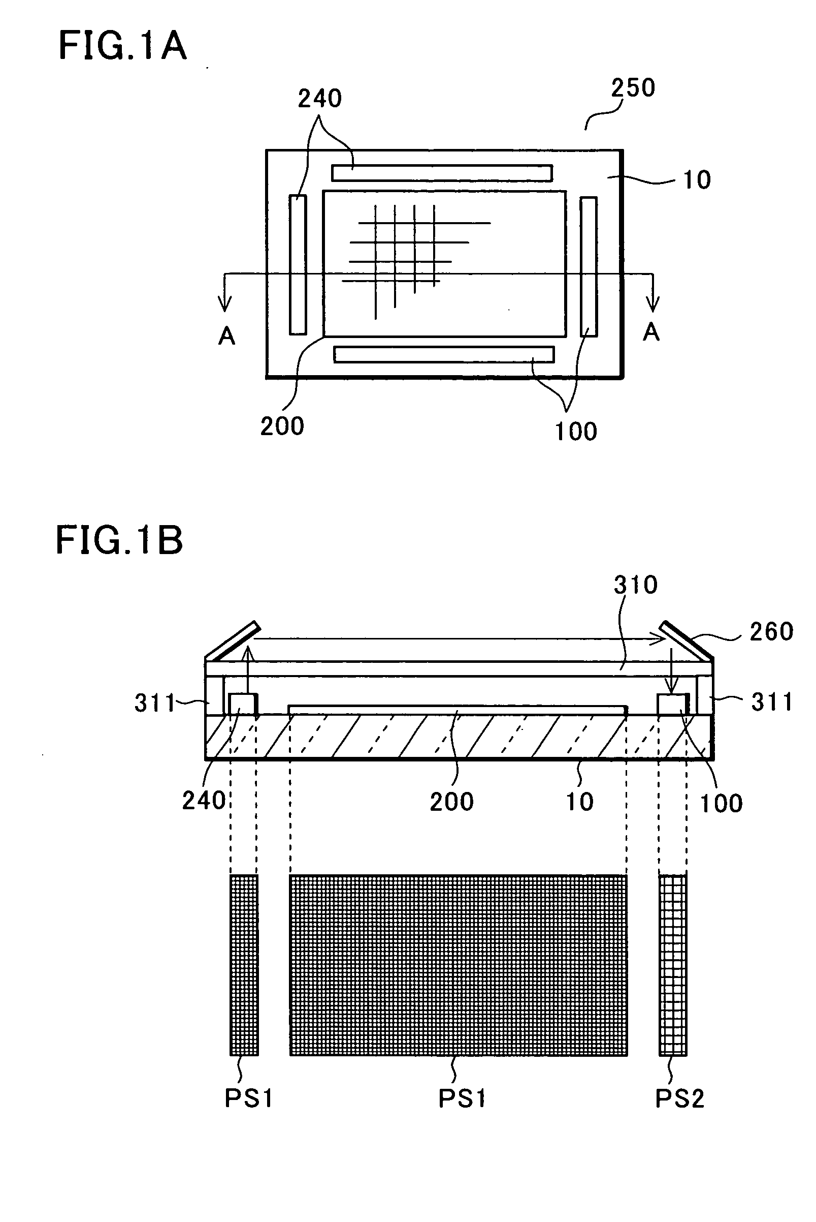
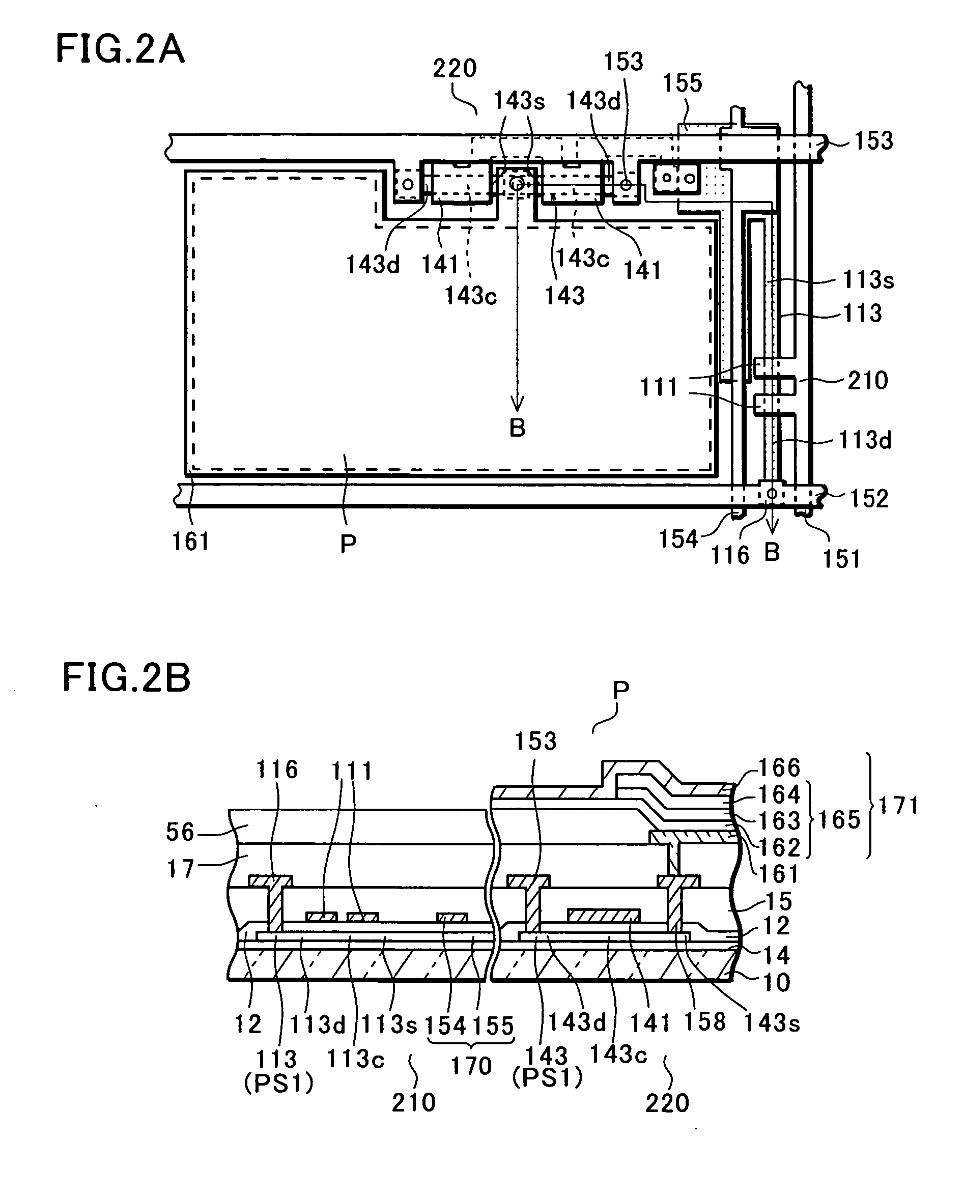
[0024] the present invention will be described with reference to FIGS. 1 though 8 in detail while taking a touch panel using an organic EL element as an example. FIG. 1A is a plan view of a touch panel, and FIG. 1B is a section view taken along the line A-A of FIG. 1A. Note that a reflection material of FIG. 1B is omitted in FIG. 1A.
[0025] Display device 250 of this embodiment of the present invention comprises photosensor 100, display portion 200 and light emission element 240, which are arranged in the same insulating substrate 10.
[0026] The display portion 200 has a switching TFT and a driving TFT, and arranges a plurality of pixels formed of an organic EL element in a matrix therein, which is connected to the driving TFT. The plurality of light emission elements 240 are arranged along two sides at the periphery of the display portion 200. The light emission elements 240 are arranged, for example, in a rectangular region of FIG. 1A at certain intervals, and the photosensors 100 ...
second embodiment
[0068] Next, a second embodiment will be described. In this embodiment of the present invention, a semiconductor layer having not only difference in the grain size of a crystal particle but also that anisotropy in a crystal length (average crystal length) may be used.
[0069] A schematic view of the device of this embodiment is the same as that in FIGS. 1 through 3, and descriptions are omitted. A method of obtaining a semiconductor layer having not only difference in the grain size of a crystal particle but also that the anisotropy in the crystal length will be described.
(1) CLC (CW-Laser Lateral Crystallization) Method
[0070] A CLC method is the one in which a DPSS (diode-pumped solid state) laser is radiated onto amorphous silicon and a crystal is grown in a scanning direction of the laser. According to this method, a crystal length of the crystal in the scanning direction is made longer by controlling a speed at which the laser is scanned.
(2) SELAX (Selectively Enlarging Laser...
PUM
 Abstract
Description
Claims
Application Information