Method of fabricating an organic electroluminescent device and system of displaying images

a technology of electroluminescent devices and images, applied in the direction of solid-state devices, semiconductor devices, thermoelectric devices, etc., can solve the problem of non-uniform luminance between pixels rendering defects such as mura, and achieve the effect of reducing the difference of electric properties and increasing the apertur

Inactive Publication Date: 2008-04-17
INNOLUX CORP
View PDF11 Cites 30 Cited by
  • Summary
  • Abstract
  • Description
  • Claims
  • Application Information

AI Technical Summary

Benefits of technology

[0007]In view of the problems in conventional processes, the addition of the protection film is proposed to decrease the difference of electric properties between TFTs. Furthermore, the aperture can be increased, even in a shorter channel length, by the addition of the protection film.

Problems solved by technology

The polysilicon TFTs (for example, serving as a driving TFT) produced by the exicimer laser annealing process, however, have various mobility, leading to a problem such as non-uniform luminance between pixels that render a defect so called mura.

Method used


Image

  • Method of fabricating an organic electroluminescent device and system of displaying images
  • Method of fabricating an organic electroluminescent device and system of displaying images
  • Method of fabricating an organic electroluminescent device and system of displaying images

Examples


first embodiment

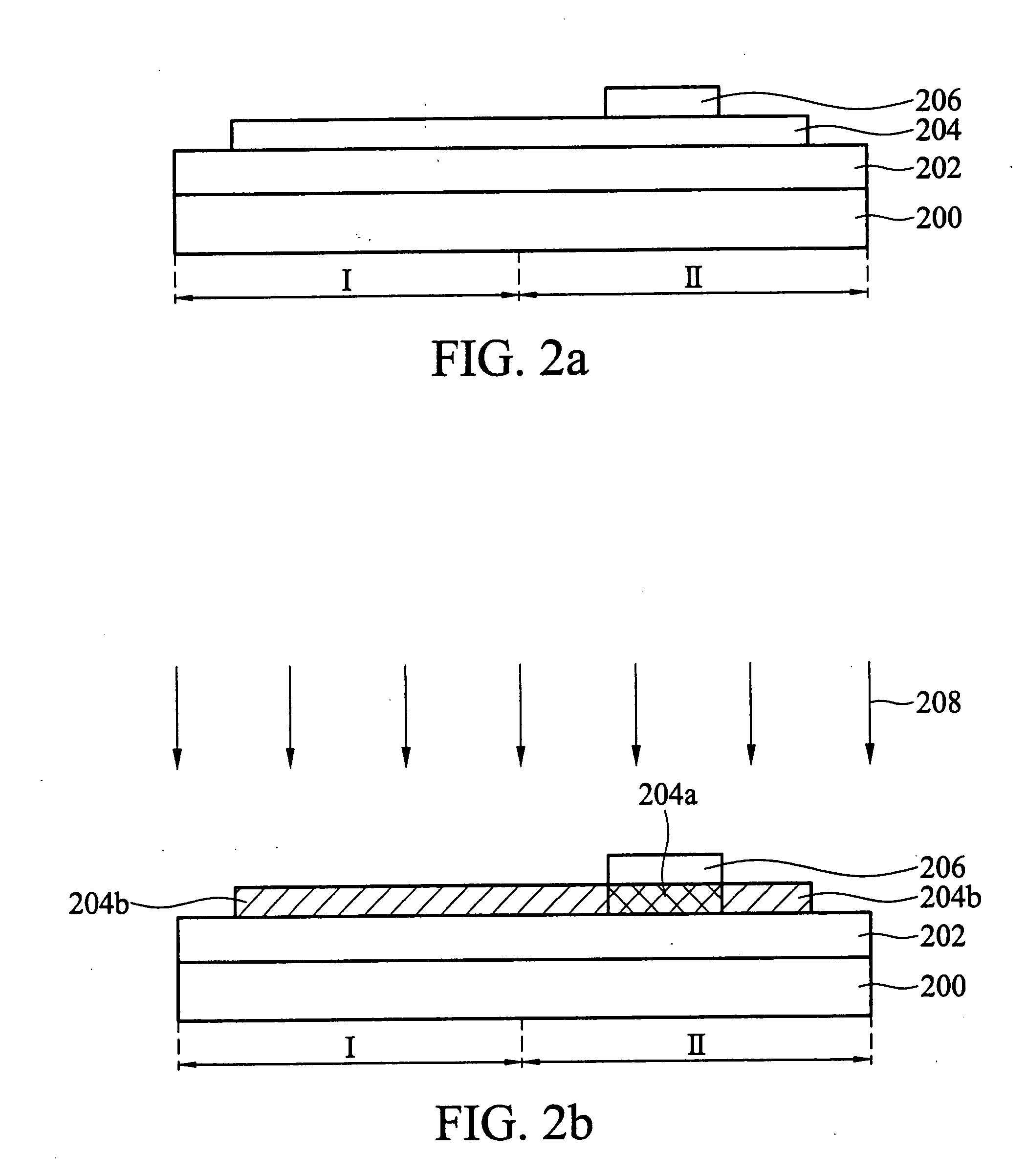
[0024]FIGS. 2a˜2f are cross sections showing an embodiment of a method for fabricating an organic electroluminescent device.

[0025]As shown in FIG. 2a, a buffer layer 202, an amorphous silicon layer 204 and a protection film 206 are formed sequentially overlying a substrate 200 divided into a first region (for example, a switching TFT region I) and a second region (for example, a driving TFT region II). The protection film 206 is formed on a portion of the amorphous silicon layer 204 in the second region II, and includes silicon-based materials such as SiOx, SiNx, SiOxNy or a stack of SiOx, SiNx.

[0026]As shown in FIG. 2b, the amorphous silicon layer 204 proceeds an excimer laser annealing (ELA) process 208 and transforms to polysilicon layers 204a and 204b. The polysilicon layers 204a and 204b, however, have different grain size because the protection film 206 can reflect a portion laser in the excimer laser annealing (ELA) process 208. That is, the polysilicon layer 204b uncovered b...

second embodiment

[0030]FIGS. 3a˜3f are cross-sections showing an embodiment of a method for fabricating an organic electroluminescent device.

[0031]As shown in FIG. 3a, a buffer layer 302 and amorphous silicon layer 304 are formed sequentially overlying a substrate 300 divided into a switching TFT region I and a driving TFT region II.

[0032]As shown in FIG. 3b, the amorphous silicon layer 304 is patterned, thus a patterned amorphous silicon layer 304b in the switching TFT region I and a patterned amorphous silicon layer 304a in the driving TFT region II are formed.

[0033]As shown in FIG. 3c, a protection film 306 is formed covering the patterned amorphous silicon layer 304a and a portion of the buffer layer 302, and includes silicon-based materials such as SiOx, SiNx, SiOxNy or a stack of SiOx, SiNx.

[0034]As shown in FIG. 3d, the patterned amorphous silicon layers 304a and 304b proceeds an excimer laser annealing (ELA) process 308 and transforms to polysilicon layers 304c and 304d. The polysilicon laye...

third embodiment

[0037]FIGS. 4a˜4g are cross sections showing an embodiment of a method for fabricating an organic electroluminescent device.

[0038]As shown in FIG. 4a, a protection film 402 is formed overlying a substrate 400 divided into a switching TFT region I and a driving TFT region II. The protection film 402 includes silicon-based materials such as SiOx, SiNx, SiOxNy or a stack of SiOx, SiNx.

[0039]As shown in FIG. 4b, a buffer layer 404 is formed overlying the patterned protection film 402 and the substrate 400. As shown in FIG. 4c, an amorphous silicon layer 406 is formed overlying the buffer layer 404.

[0040]As shown in FIG. 4d, the amorphous silicon layer 406 proceeds an excimer laser annealing (ELA) process 408 and transforms to polysilicon layers 406a and 406b.

[0041]As shown in FIG. 4e, patterned polysilicon layers 406′a and 406b are formed after a patterning process of the polysilicon layers 406a and 406b. The polysilicon layers 406′a in the switching TFT region I serves a first active ...


PUM

PropertyMeasurementUnit
areaaaaaaaaaaa
grain sizeaaaaaaaaaa
thermal conductivityaaaaaaaaaa

Abstract

A method for fabricating organic electroluminescent devices is disclosed. The method comprises providing a substrate divided into first and second regions, forming an amorphous silicon layer on the substrate, forming a protection film on the amorphous silicon layer within the second region, performing an excimer laser annealing process on the amorphous silicon layer for converting it to a polysilicon layer, removing the protection film, patterning the polysilicon layer, thus a first patterned polysilicon layer in the first region and a second patterned polysilicon layer in the second region are formed. A resultant organic electroluminescent device is obtained. Specifically, the grain size of the first patterned polysilicon layer is large than that of the second patterned polysilicon layer.

Description

BACKGROUND OF THE INVENTION[0001]1. Field of the Invention[0002]The present invention relates to a method for fabricating an electroluminescent device, and in particular relates to a method for fabricating a thin film transistor (TFT).[0003]2. Description of the Related Art[0004]A conventional thin film transistor (TFT), can be an amorphous silicon TFT or a polysilicon silicon TFT, includes light emitting and circuit regions. A fabrication method thereof mainly includes the steps of forming TFTs, forming a pixel electrode and forming organic light emitting diodes. Fabrication processes of a TFT typically include forming buffer layer, polysilicon layer, gate insulating layer, gate electrode and interlayer dielectric overlying the overall substrate surface in sequence. A pixel electrode electrically connected to the TFTs is then formed after the completion of the TFTs. Thereafter, a resultant electroluminescent device is obtained by sequential formation of transparent electrode, organ...

Claims


Application Information

Patent Timeline
Patent Type & Authority Applications(United States)
IPC IPC(8): H01L51/50H01L21/336
CPCH01L27/1229H01L27/1281H01L27/1237H01L27/1296
Inventor CHAN, CHUAN-YILIU, CHUN-YENTSENG, CHANG-HO
Owner INNOLUX CORP
Why Eureka
Try Eureka