Cathode cell design

a cathode cell and cathode technology, applied in the direction of semiconductor devices, basic electric elements, electrical equipment, etc., can solve the problems of not meeting, devices will experience harsher soa conditions, and the rbsoa becomes more critical, so as to increase the cell latch-up immunity, and reduce the on-state loss

Active Publication Date: 2008-04-17
HITACHI ENERGY SWITZERLAND AG
View PDF14 Cites 2 Cited by
  • Summary
  • Abstract
  • Description
  • Claims
  • Application Information

AI Technical Summary

Benefits of technology

[0007] It is an object of the invention to provide a power insulated gate semiconductor device of the initially mentioned kind with an increased SOA (safe operating area) and low on-state losses.
[0019] In a preferred embodiment, no region of the second conductivity type with a doping density higher than the channel well region is arranged in the active cell, thus on-state losses are reduced.
[0020] The third layer in an insulated gate semiconductor device according to the invention reduces the on-state losses by having a low hole drain effect by providing a hole barrier region. The hole barrier effect in the third layer will also increase the cell latch-up immunity in the active cell regions. The additional well regions provide an avalanche point away from the active cell peripheries, and an alternative path for the holes away from the critical source regions. The additional well regions do not affect the active cell design in terms of cell pitch, i.e. the design rules for the distance between the active cells, and hole drainage between the cells, hence resulting in optimum carrier profile at the emitter side having low on-state losses.

Problems solved by technology

For high voltage devices, the RBSOA becomes more critical due to the low n-base doping levels and associated dynamic avalanche, which will occur at lower current densities.
Also, such devices will experience much harsher SOA conditions at high DC link voltages during testing and operation.
However, it is well known that the standard approach mentioned above will not fulfil the SOA requirements especially when designing IGBTs with ratings ranging from 2000 V up to 8000 V. In addition, there is a design trade-off between improved safe operating area using additional p+ well regions and reduced on-state losses for the high voltage IGBT.
However for high voltage IGBTs with ratings exceeding 2000 V, such an IGBT has shown not to be effective for increasing the SOA capability sufficiently.

Method used


Image

  • Cathode cell design
  • Cathode cell design
  • Cathode cell design

Examples


Embodiment Construction

[0007] It is an object of the invention to provide a power insulated gate semiconductor device of the initially mentioned kind with an increased SOA (safe operating area) and low on-state losses.

[0008] This object is achieved by an IGBT according to the independent claims.

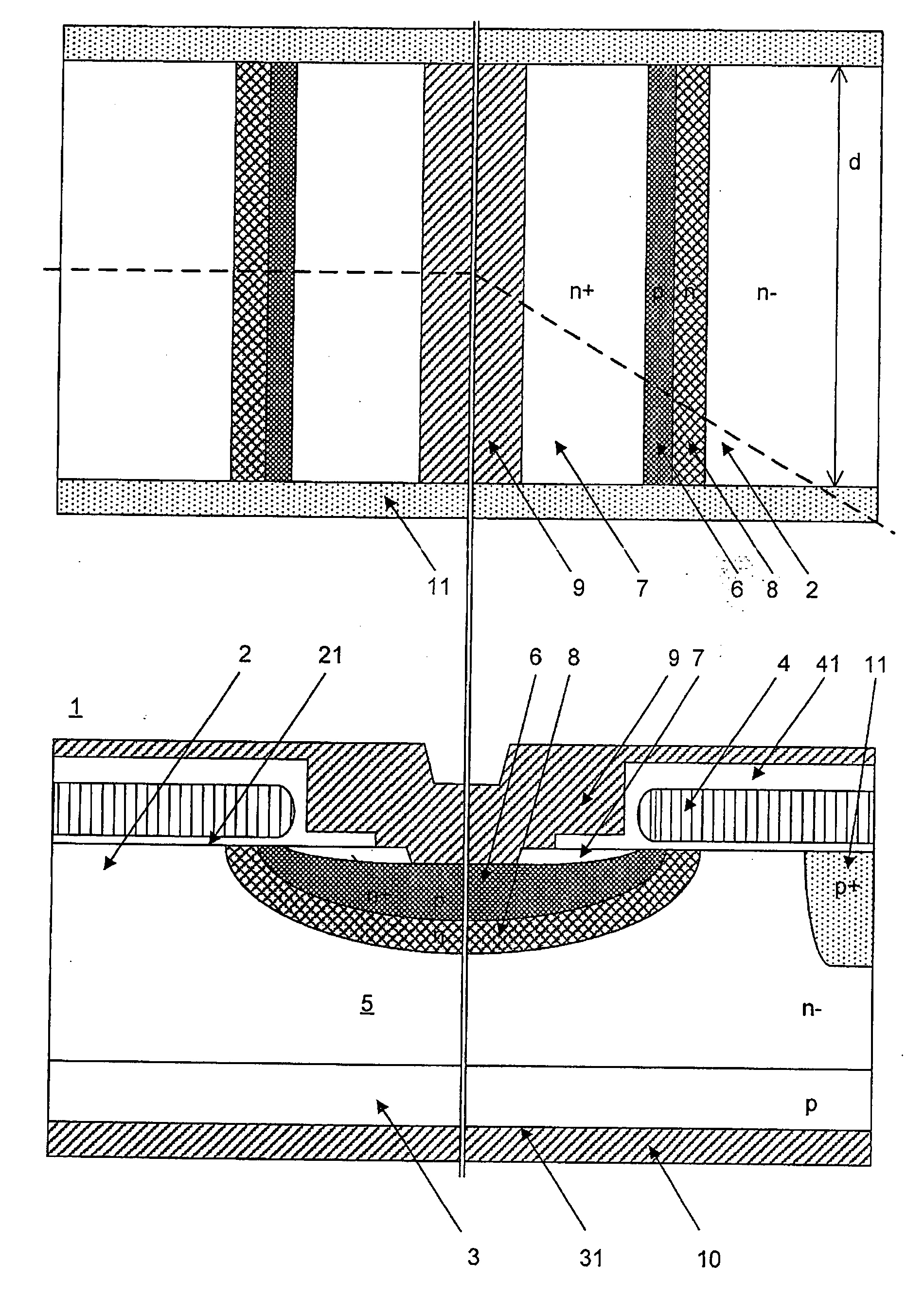
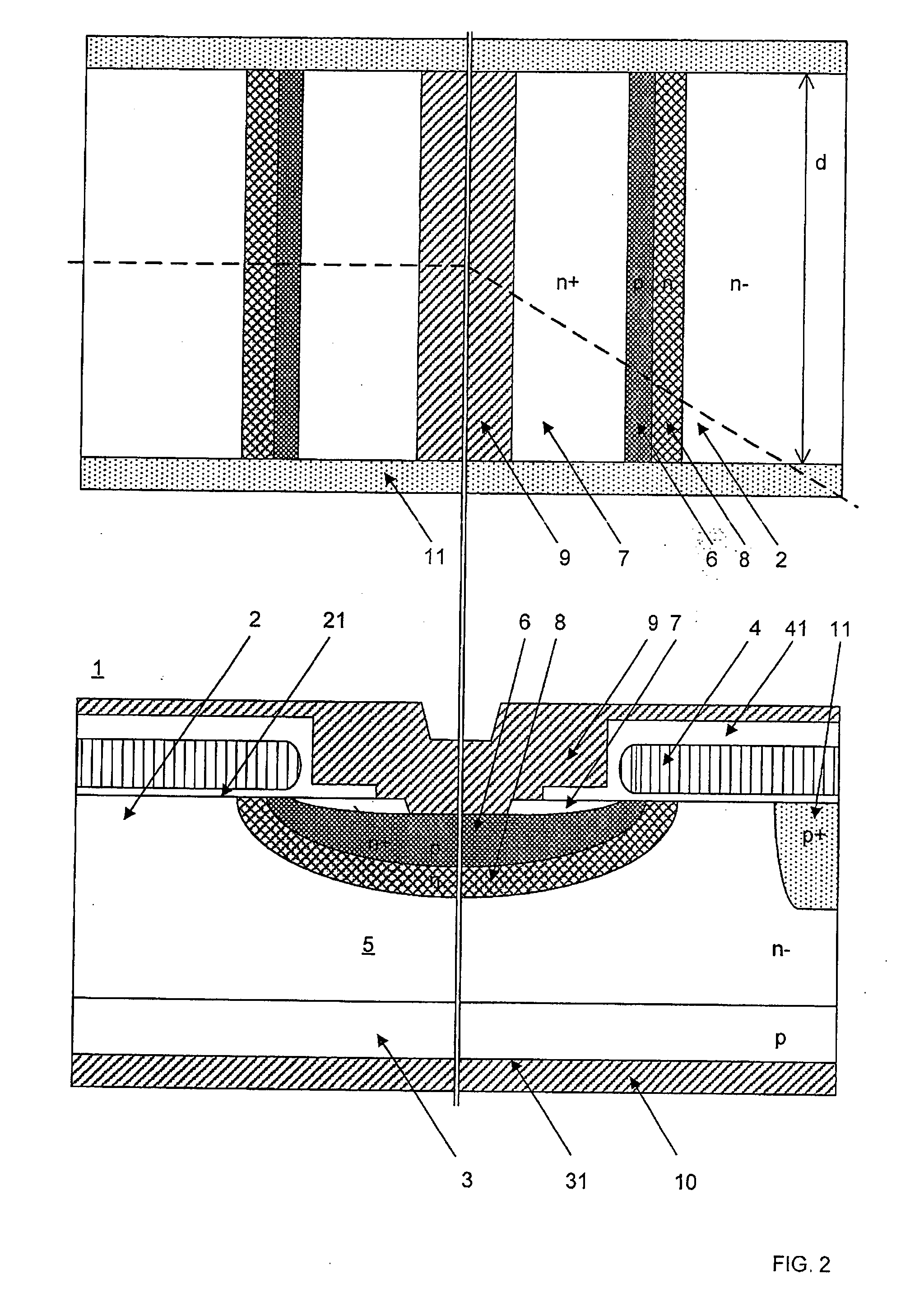
[0009] An insulated gate semiconductor device according to the invention comprises a first layer of a first conductivity type with an upper side. Insulated gate electrodes are formed on the upper side. The semiconductor device further comprising an active semiconductor cell, which comprises [0010] a part of the first layer and [0011] a channel well region of the second conductivity type, [0012] source regions of the first conductivity type having a doping density higher than said first layer, [0013] a third layer of the first conductivity type having a doping density higher than the first layer, and lower than the doping density of the source regions, and [0014] emitter electrodes which are formed on the upper si...


PUM


Abstract

An n-channel insulated gate semiconductor device with an active cell (5) comprising a p channel well region (6) surrounded by an n type third layer (8), the device further comprising additional well regions (11) formed adjacent to the channel well region (6) outside the active semiconductor cell (5) has enhanced safe operating are capability. The additional well regions (11) outside the active cell (5) do not affect the active cell design in terms of cell pitch, i.e. the design rules for cell spacing, and hole drainage between the cells, hence resulting in optimum carrier profile at the emitter side for low on-state losses.

Description

FIELD OF THE INVENTION [0001] The invention relates to the field of high voltage power semiconductor devices. It relates to a power insulated gate semiconductor device according to the preamble of independent claims. BACKGROUND OF THE INVENTION [0002] The safe operating area (SOA) of a power semiconductor device is a graphical representation of the maximum operational voltage and current limits of the device subjected to various constraints. The forward bias safe operating area (FBSOA) and the reverse bias safe operating area (RBSOA) represent the device SOA with the gate-emitter forward biased or reverse biased, respectively. [0003] For high voltage devices, the RBSOA becomes more critical due to the low n-base doping levels and associated dynamic avalanche, which will occur at lower current densities. Also, such devices will experience much harsher SOA conditions at high DC link voltages during testing and operation. [0004] Standard planar Insulated-Gate Bipolar Transistor (IGBT) ...

Claims


Application Information

Patent Timeline
Patent Type & Authority Applications(United States)
IPC IPC(8): H01L29/76H01L21/336
CPCH01L29/7395H01L29/0696
Inventor RAHIMO, MUNAF
Owner HITACHI ENERGY SWITZERLAND AG
Why Eureka
Try Eureka