Semiconductor package structure and method of fabricating the same

a technology of semiconductors and packaging, applied in the direction of semiconductor devices, semiconductor/solid-state device details, electrical devices, etc., can solve the problems of undesirable increase of cost and time associated with fabricating pops, deterioration of packaging process flexibility, etc., to improve the flexibility the effect of easy change of the structure of the chip selection uni

Active Publication Date: 2008-04-17
SAMSUNG ELECTRONICS CO LTD
View PDF11 Cites 39 Cited by
  • Summary
  • Abstract
  • Description
  • Claims
  • Application Information

AI Technical Summary

Benefits of technology

[0016] The present invention provides a semiconductor package structure that can easily change the structure of a chip selection unit. Also, the present invention provides a method of fabricating a semiconductor package structure that can improve the flexibility of the structure of a chip selection unit.

Problems solved by technology

However, determining the structure of each of the chip selection units 90 in the chip designing process tends to deteriorate the flexibility of the packaging process.
As a result, it is not easy to change the chip designing process for various reasons.
As a result, the cost and time associated with fabricating a PoP may be undesirably increased.
Furthermore, even if the semiconductor chips C1 to C4 are of the same configuration, the stacked order of the semiconductor chips C1 to C4 cannot be arbitrarily changed due to the fixed structures of the chip selection units 90.
Thus, in the event that there is a supply shortage of a particular semiconductor chip, shipment of PoP devices incorporating the particular semiconductor chip may be delayed.

Method used


Image

  • Semiconductor package structure and method of fabricating the same
  • Semiconductor package structure and method of fabricating the same
  • Semiconductor package structure and method of fabricating the same

Examples


Embodiment Construction

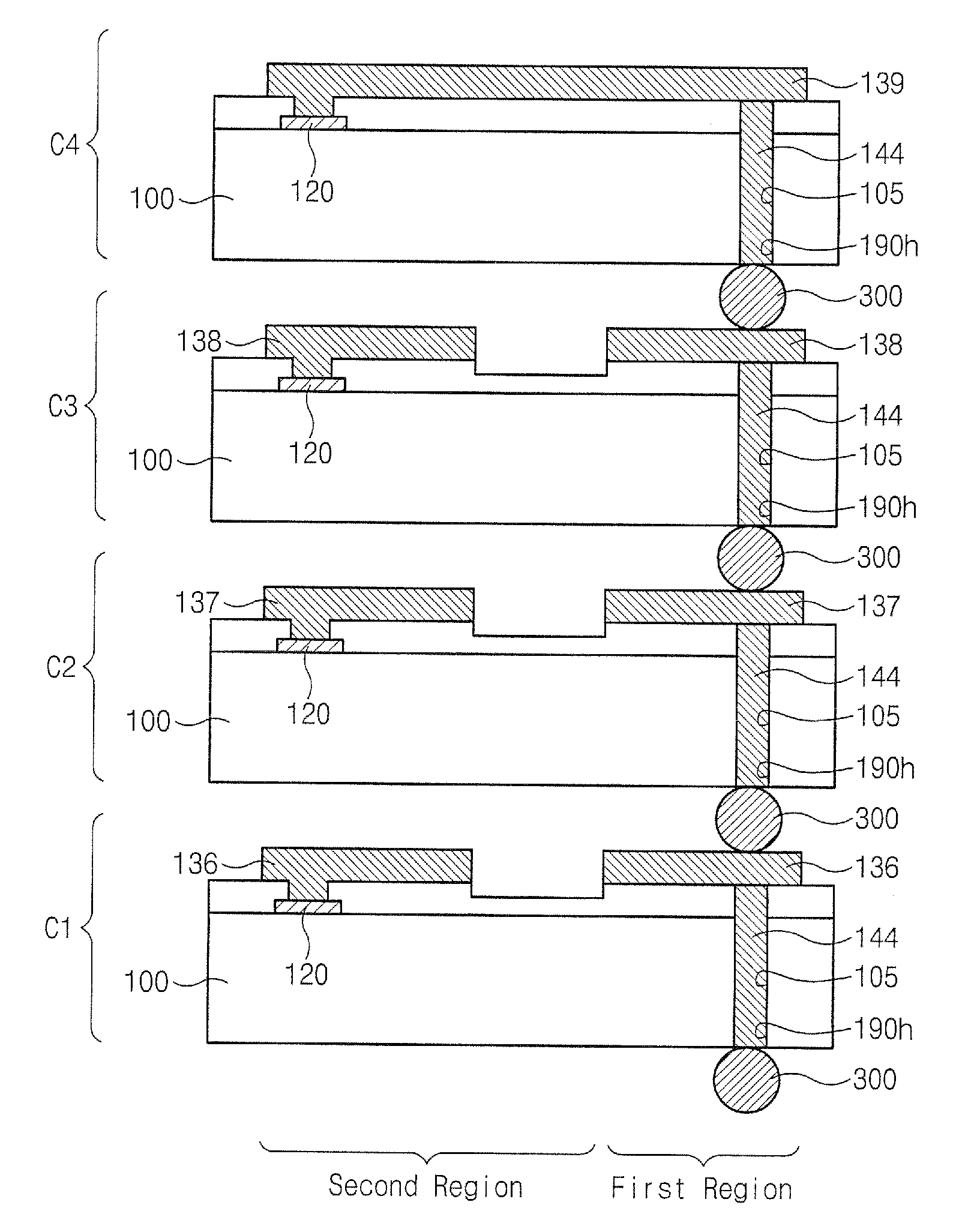
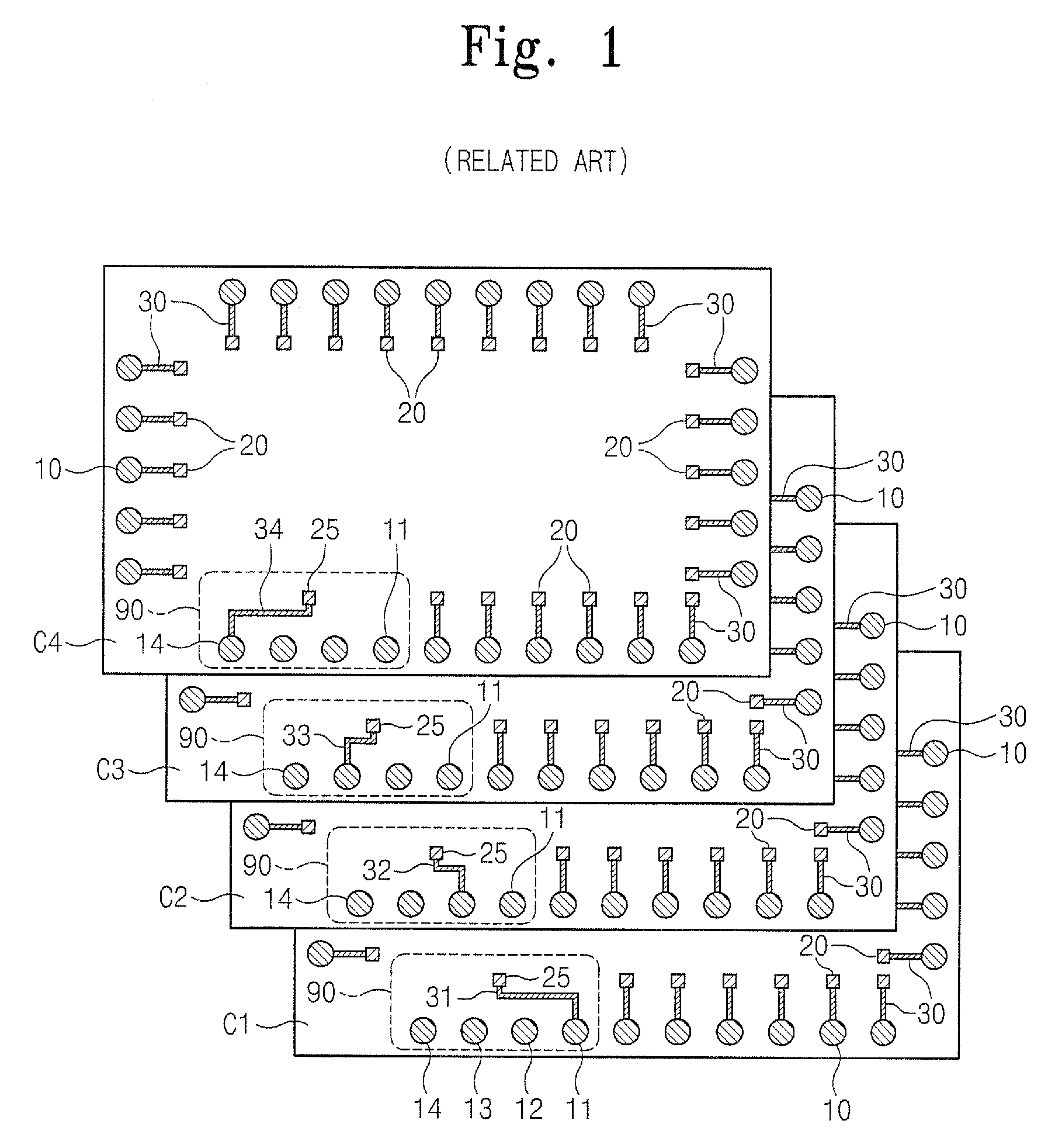
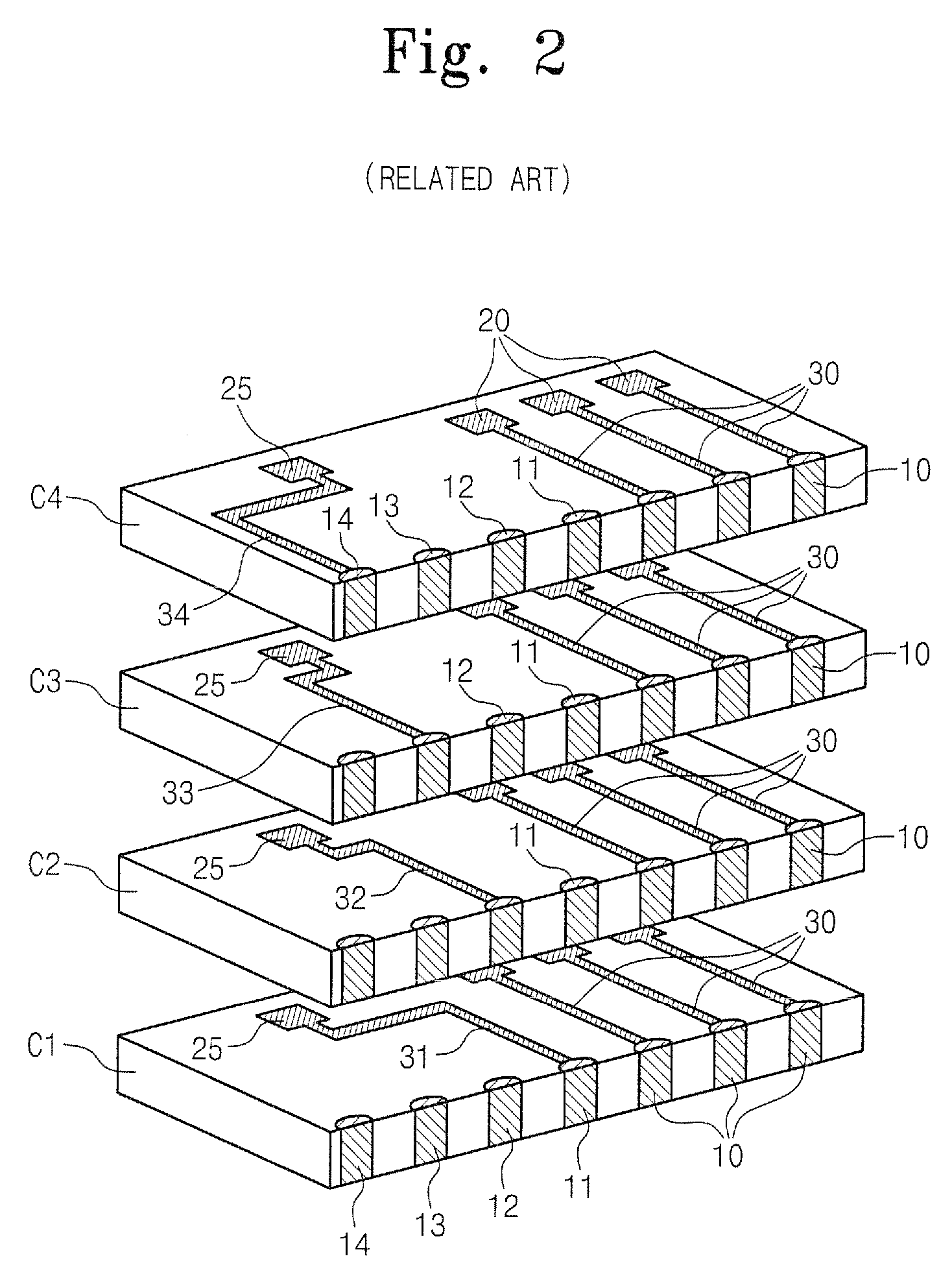
[0026] Reference will now be made in detail to the embodiments of the present invention, examples of which are illustrated in the accompanying drawings. However, the embodiments are not limited to the description provided below, and the embodiments herein are rather introduced to provide easy and complete understanding of the scope and spirit of the present invention.

[0027] It will also be understood that when a layer is referred to as being “on” another layer or substrate, it can be directly on the other layer or substrate, or intervening layers may also be present. In the drawings, the thicknesses of layers and regions are exaggerated for clarity. It will be understood that although the terms first and second are used herein to describe various regions, layers and / or sections should not be limited by these terms. These terms are only used to distinguish one region, layer or section from another region, layer or section. Thus, for example, a first layer discussed below could be te...


PUM


Abstract

A semiconductor package structure and a method of fabricating the same are disclosed. A method of fabricating the semiconductor package structure can be characterized as including forming semiconductor chips on a semiconductor substrate. Each of the semiconductor chips includes chip pads. Through-vias are formed through the semiconductor chips. Redistribution structures and a chip selection interconnection layer are formed on the semiconductor chips, which connect the through-vias with the chip pads. The chip selection interconnection layers are patterned to form chip selection interconnection lines having different structures on at least one of the semiconductor chips. The semiconductor chips are stacked and electrically connected using the through-vias.

Description

CROSS-REFERENCE TO RELATED APPLICATION [0001] This application claims the benefit of foreign priority to Korean Patent Application No. 10-2006-0097474, filed on Oct. 3, 2006, the disclosure of which is hereby incorporated by reference herein in its entirety. BACKGROUND [0002] 1. Field of Invention [0003] Embodiments of the present invention generally relate to semiconductor package structures and methods of fabricating the same. More particularly, embodiments of the present invention relate to a semiconductor package structure and a method of fabricating the same which facilitates changing the design of a structure of a chip selection unit. [0004] 2. Description of the Related Art [0005] A semiconductor fabrication process includes a front-end process for fabricating integrated circuit (IC) chips on a wafer using photolithography, deposition, and etching processes and a back-end process for assembling and packaging the respective IC chips. Four significant functions of the packaging...

Claims


Application Information

Patent Timeline
Patent Type & Authority Applications(United States)
IPC IPC(8): H01L23/48H01L21/60
CPCH01L25/0657H01L25/50H01L2224/16145H01L2225/06513H01L23/5258H01L2225/06541H01L2225/06555H01L23/481H01L2225/06527H01L24/03H01L24/05H01L24/11H01L24/13H01L24/16H01L2224/0231H01L2224/02371H01L2224/02372H01L2224/04105H01L2224/05001H01L2224/05008H01L2224/05009H01L2224/05022H01L2224/05025H01L2224/05548H01L2224/05569H01L2224/0615H01L2224/13008H01L2224/13025H01L2224/16146H01L2224/16148H01L2924/00014H01L2224/05599H01L2224/05099H01L23/12
Inventor KWON, YONG-CHAILEE, DONG-HO
Owner SAMSUNG ELECTRONICS CO LTD
Why Eureka
Try Eureka