Lateral power MOSFET with high breakdown voltage and low on-resistance

a technology of lateral power mosfet and low breakdown voltage, which is applied in the direction of semiconductor devices, basic electric elements, electrical equipment, etc., can solve the problems of low breakdown voltage, inability to maintain a low on-resistance, and less efficient devices

Active Publication Date: 2008-04-17
TAIWAN SEMICON MFG CO LTD
View PDF3 Cites 32 Cited by
  • Summary
  • Abstract
  • Description
  • Claims
  • Application Information

AI Technical Summary

Problems solved by technology

A problem with this type of lateral power MOSFET is that it cannot maintain a low on-resistance when a high voltage is passed through the lateral power MOSFET.
The larger the on-resistance of the device, the less efficient the device.
Another problem with the prior art device 100 (shown in FIG. 1A) and the prior art device 150 (shown in FIG. 1B) is that the breakdown voltage is not as high as desired.
When voltage larger than the breakdown voltage is passed through devices such as device 100 and device 150, catastrophic and irreversible damage is done to the devices, rendering the devices commercially useless and requiring the devices to be replaced.
Those prior art systems, however, have difficulties sustaining high voltage and low on-resistance, thus, an improved lateral power MOSFET is needed for a reduced on-resistance and a higher breakdown voltage when the device is placed under a high voltage.

Method used


Image

  • Lateral power MOSFET with high breakdown voltage and low on-resistance
  • Lateral power MOSFET with high breakdown voltage and low on-resistance
  • Lateral power MOSFET with high breakdown voltage and low on-resistance

Examples


Embodiment Construction

[0022]The making and using of the presently preferred embodiments are discussed in detail below. It should be appreciated, however, that the present invention provides many applicable inventive concepts that can be embodied in a wide variety of specific contexts. The specific embodiments discussed are merely illustrative of specific ways to make and use the invention, and do not limit the scope of the invention.

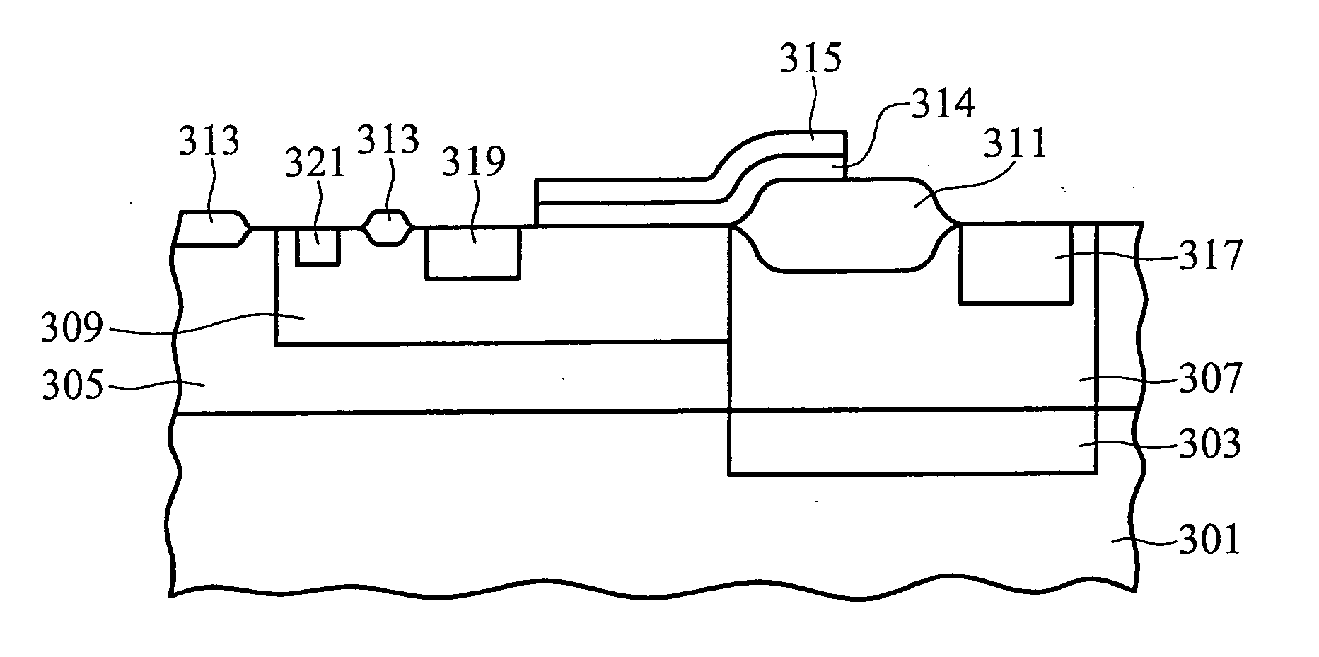
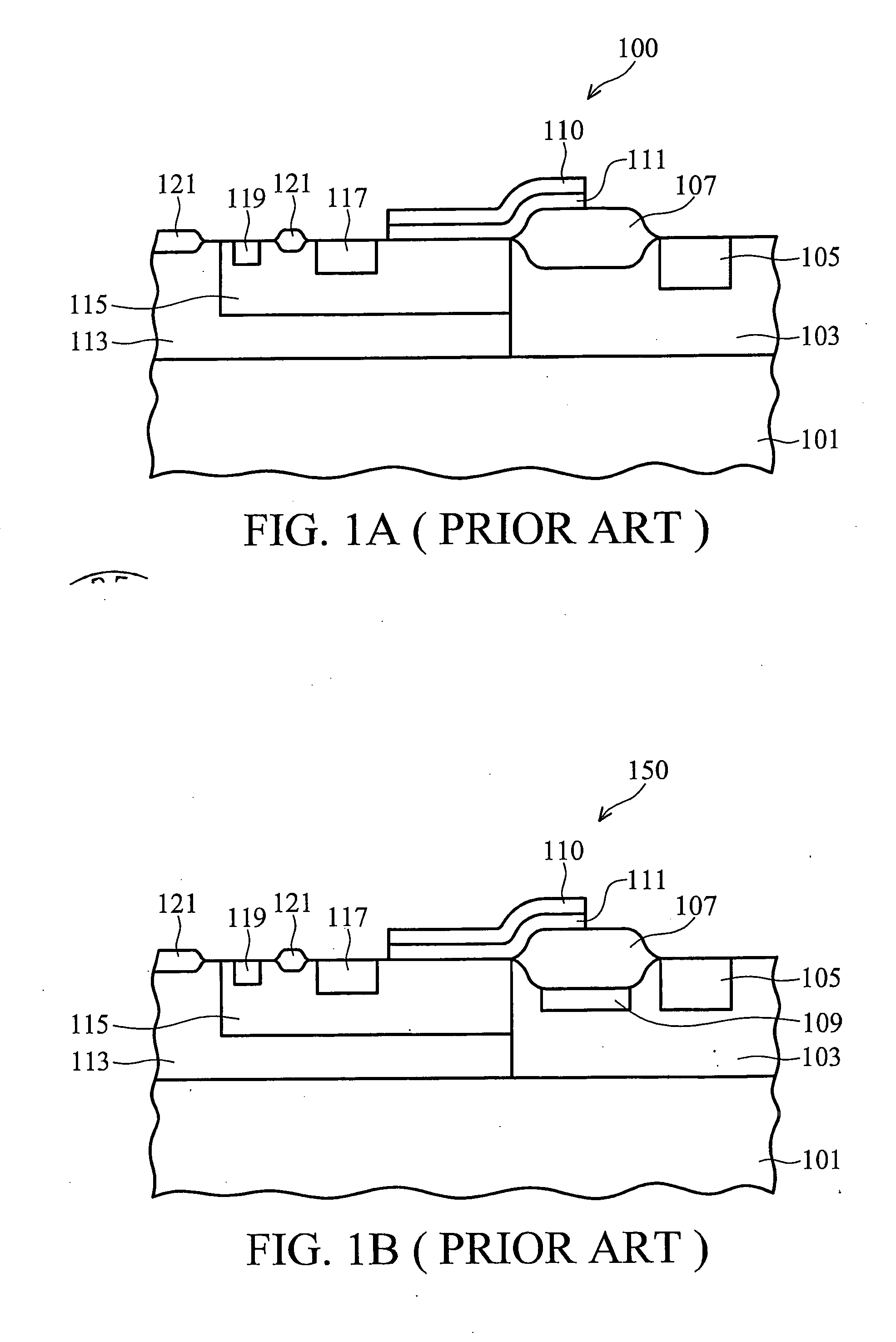
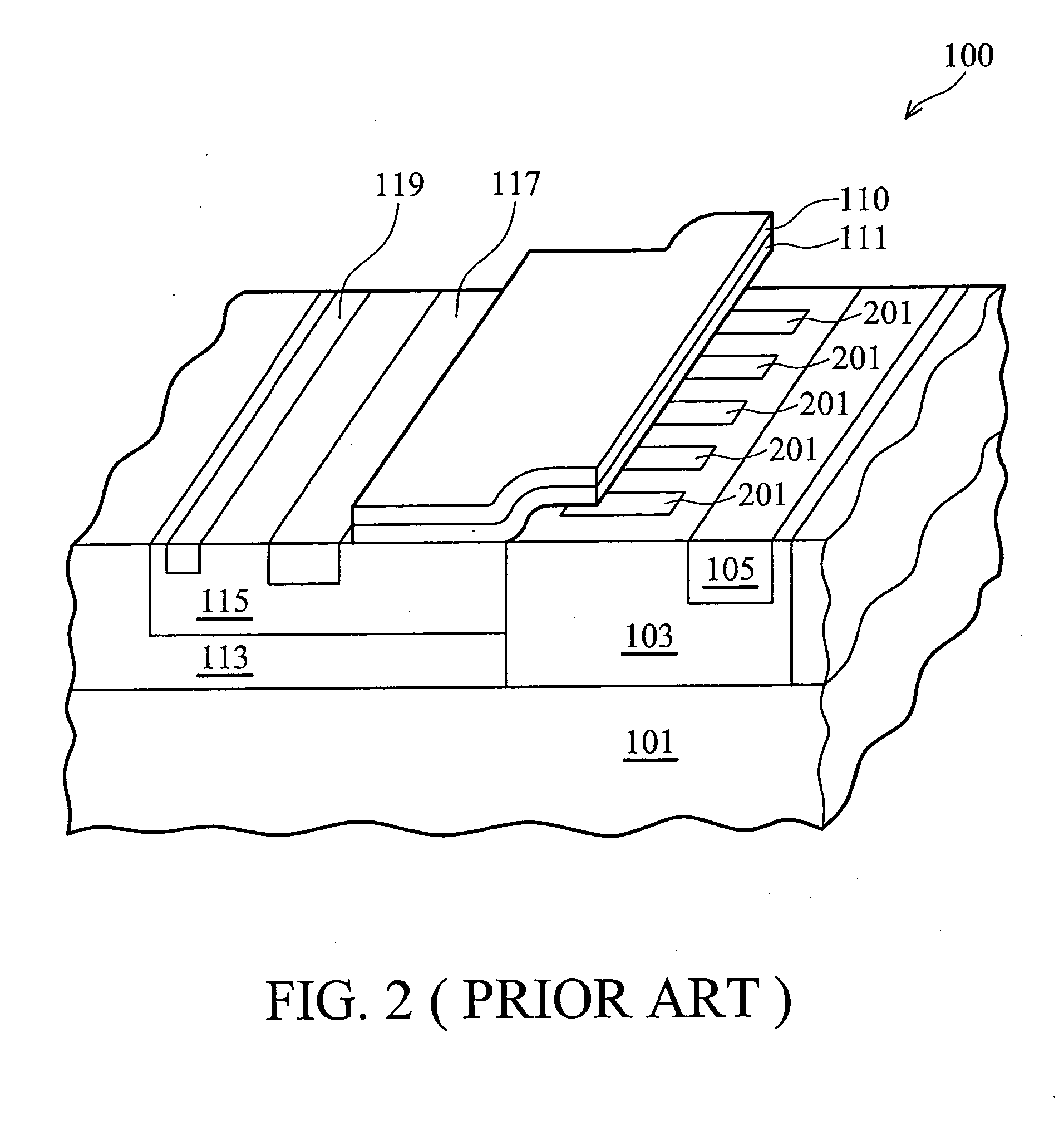
[0023]The present invention is a semiconductor device with a reduced on-resistance and an increased breakdown voltage when the device is under a large voltage. Embodiments of the present invention may be useful for lateral power MOSFETs, particularly when the device is under a large voltage. In an embodiment discussed herein, a voltage of about 800 V is large. However, voltages greater than or less than 800 V may be considered large in other embodiments of the present invention. The manufacturing process of this device is detailed in the following paragraphs.

[0024]Referring f...


PUM


Abstract

A semiconductor device with high breakdown voltage and low on-resistance is provided. An embodiment comprises a substrate having a buried layer in a portion of the top region of the substrate in order to extend the drift region. A layer is formed over the buried layer and the substrate, and high-voltage N-well and P-well regions are formed adjacent to each other. Field dielectrics are located over portions of the high-voltage N-wells and P-wells, and a gate dielectric and a gate conductor are formed over the channel region between the high-voltage P-well and the high-voltage N-well. Source and drain regions for the transistor are located in the high-voltage P-well and high-voltage N-well. Optionally, a P field ring is formed in the N-well region under the field dielectric. In another embodiment, a lateral power superjunction MOSFET with partition regions located in the high-voltage N-well is manufactured with an extended drift region.

Description

TECHNICAL FIELD[0001]This invention relates generally to semiconductor structures and methods, and more particularly to a lateral power metal oxide semiconductor field effect transistor (MOSFET).BACKGROUND[0002]A lateral power MOSFET is basically a metal oxide semiconductor field effect transistor fabricated with coplanar drain and source regions. FIG. 1A shows a lateral power MOSFET device 100 in the prior art. The device 100 is formed on a p-type substrate 101 and another p-layer 113 is epitaxially grown on the substrate 101. A high-voltage P-well 115 is adjacent a high-voltage N-well 103 in the epitaxially grown p-layer 113. An N+ source 117 is positioned in the high-voltage P-well 115 such that the N+ source 117 is not immediately adjacent the high-voltage N-well 103, and an N+ drain 105 is positioned in the high-voltage N-well 103. Dielectrics 121 are formed to isolate and define areas such as the N+ source 117 and the N+ drain 105 of the device 100. A gate dielectric 111 and a...

Claims


Application Information

Patent Timeline
Patent Type & Authority Applications(United States)
IPC IPC(8): H01L21/8234H01L21/336
CPCH01L29/063H01L29/0634H01L29/7835H01L29/42368H01L29/66659H01L29/0847H01L29/0878H01L21/18
Inventor HUANG, TSUNG-YICHIANG, PUO-YULIU, RUEY-HSINHSU, SHUN-LIANG
Owner TAIWAN SEMICON MFG CO LTD
Why Eureka
Try Eureka