Semiconductor device and method of manufacturing the same

a semiconductor and semiconductor technology, applied in the field of systemonachip (soc) semiconductor devices, can solve the problems of increasing junction leak current and achieve the effects of reducing manufacturing processes, preventing junction leakage, and reducing carrier mobility

Inactive Publication Date: 2008-04-24
NEC ELECTRONICS CORP
View PDF2 Cites 29 Cited by
  • Summary
  • Abstract
  • Description
  • Claims
  • Application Information

AI Technical Summary

Benefits of technology

[0019] On the other hand, in the case of using the work function control using hafnium, the channel dose can be reduced to 5.3×10¹² (atoms / cm2), thereby making it possible to reduce the threshold difference in association with the transistor width W due to the reverse narrow channel effect.
[0034] In addition, since the channel dose is suppressed to be small, undesired degradation of characteristics, such as, reduction in carrier mobility and increase of junction leak can be prevented.

Problems solved by technology

As a result, problems such as decrease of a carrier mobility and increase of a junction leak current remain unsolved.

Method used


Image

  • Semiconductor device and method of manufacturing the same
  • Semiconductor device and method of manufacturing the same
  • Semiconductor device and method of manufacturing the same

Examples


Embodiment Construction

[0050] Hereinafter, an embodiment of the present invention will be described in detail with reference to the drawings and tables.

[0051]FIG. 7 shows a structure of functional blocks provided on an SoC semiconductor chip according to the embodiment of the present invention. The SoC includes a logic portion 10 including a plurality of logic transistors, an SRAM 20 including a plurality of memory cell transistors and peripheral transistors, and an I / O 30 including a plurality of I / O transistors. In the SoC, a plurality of power supply voltages are used. For example, the power supply voltage of each of the logic portion 10 and the SRAM 20 is 1.2 V, and the power supply voltage of the I / O 30 is 1.8 V and 3.3 V.

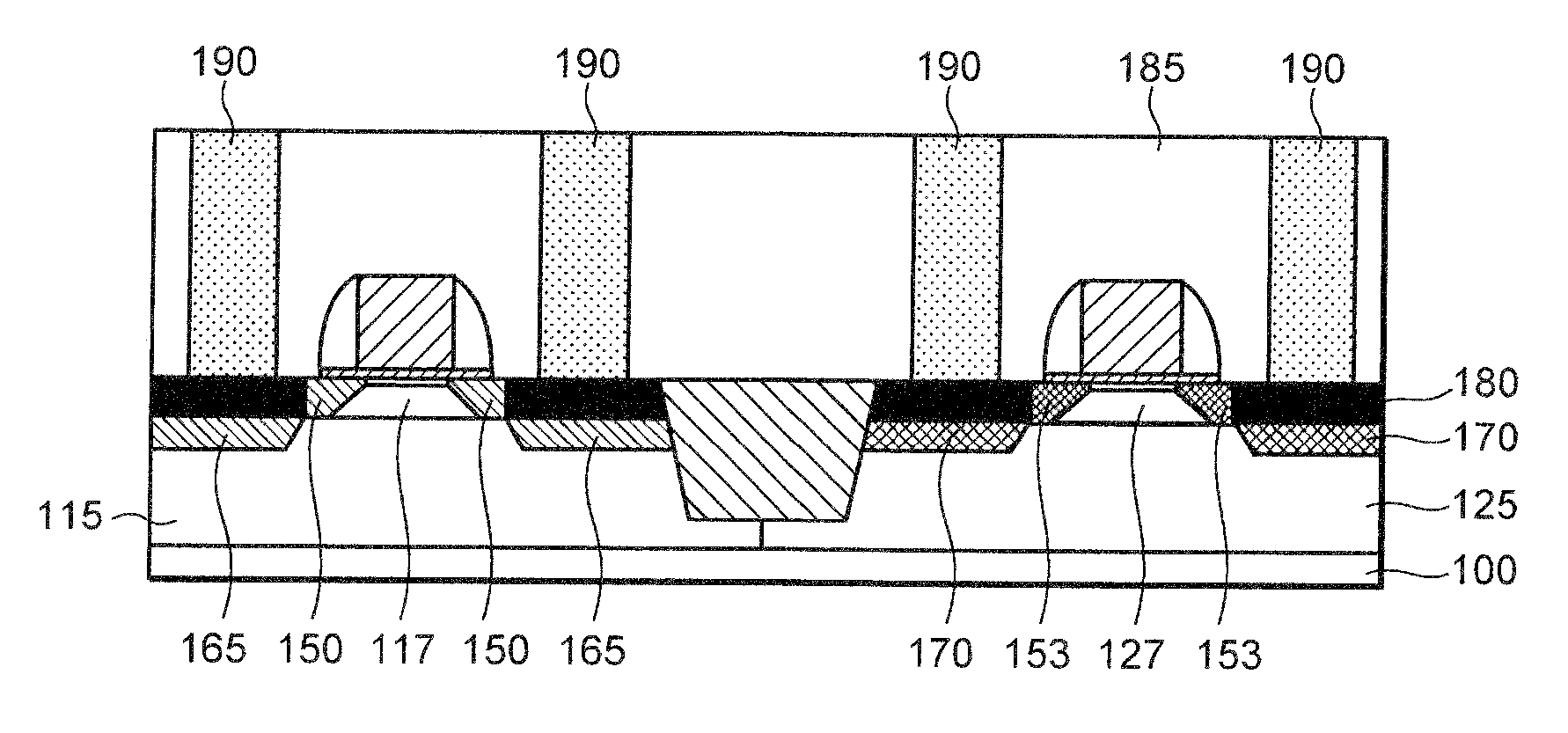
[0052]FIGS. 8A to 8C each show a schematic plan view and a cross-sectional view of a typical transistor which is formed on the SoC. FIG. 8A shows a logic transistor (also referred to as “core transistor”) which is used in the logic portion 10, is formed on a semiconductor substrat...


PUM


Abstract

The semiconductor device includes a plurality of transistors at least having different channel widths from each other. Threshold voltages of those transistors are set to be substantially equal to each other, by using both of substantially the same channel dose for each of those transistors, and work function control using a predetermined metal to be deposited on a gate insulating of those transistors and / or a gate electrode material of each of those transistors (that is, work function control based on a gate structure (gate insulating film and / or gate electrode) with respect to a channel region of each of those transistors).

Description

BACKGROUND OF THE INVENTION [0001] 1. Field of the Invention [0002] The present invention relates to a system-on-a-chip (SoC) semiconductor device, and a method of manufacturing the same. In particular, the present invention relates to threshold voltage control for transistors provided on an SoC. [0003] 2. Description of the Related Art [0004] A threshold voltage of a transistor has a considerable effect on electrical characteristics such as an operating speed and a leak current. Accordingly, it is necessary to set the threshold voltage so as to obtain desired characteristics. The threshold voltage of a transistor depends on an impurity concentration of a channel region. Therefore, by controlling an amount of impurities to be doped into the channel region (channel dose), it is possible to control the threshold voltage (for example, see JP 2001-267431 A). JP 2001-267431 A also discloses that controlling of a planar shape of a portion to be doped with impurities while setting the chan...

Claims


Application Information

Patent Timeline
Patent Type & Authority Applications(United States)
IPC IPC(8): H01L29/00
CPCH01L21/2652H01L21/82385H01L27/0207H01L29/105H01L27/11H01L27/1116H01L27/105H10B10/00H10B10/18
Inventor ABE, TOMOHISATSUTSUI, GENFUKASE, TADASHINAKAHARA, YASUSHIIMAI, KIYOTAKA
Owner NEC ELECTRONICS CORP
Why Eureka
Try Eureka