
Layout structure

Inactive Publication Date: 2008-05-01
INFINEON TECH AG
View PDF7 Cites 0 Cited by
  • Summary
  • Abstract
  • Description
  • Claims
  • Application Information

AI Technical Summary

Benefits of technology

[0007]An embodiment of the present invention provides a layout structure (e.g. a coupling structure) with a conducting line (e.g. a metal line) extending in a conducting line direction, the conducting line being arranged within a substrate area, a fill element being arranged within the substrate area at a predetermined distance from the conducting line, the fill element having a fill element axis extending perpendicularly to a side (e.g. to a straight line formed by the side) of the fill element in a fill element direction, an angle between the conducting line direction and the fill element direction being greater than 0° and smaller than 90°. Therefore, the coupling capacity between the fill elements and the conducting line is reduced.
[0018]A hole or hole structures in a conducting line (e.g. metal line) may improve the manufacturing process with respect to e.g. wide metal lines, since the holes in the metal line provide for a uniform “metal” density. The more uniform the density is the better is the result of a smoothing process based on e.g. CMP (Chemical Mechanical Polishing). Although the holes may be placed orthogonally with respect to a current flow, it is advantageous to rotate the holes within the line by e.g. 45° which improves a functionality of the line without adversely affecting the manufacturing process. The advantages with respect to an electrical functionality result from the fact that the profile of the line is not significantly reduced so that higher current amplitudes are possible and that at the same current force a higher reliability may be obtained, respectively.
[0034]The fill pattern can be placed closer to e.g. an active shape so that an improved density distribution and / or a reduced coupling capacity can be achieved. Therefore, by way of example, the interconnect capacity is negligible for 99% of nets and does not need to be considered during the implementation process.

Problems solved by technology

Unfortunately, a conductive fill pattern increases an interconnect (coupling) capacity which leads to an increased cross and noise coupling and therefore reduces the circuit performance and makes a timing sign-off difficult.
Unfortunately, the coupling capacity would increase even more in that case.
Thus, although a higher density is achievable due to smaller fill shapes, the introduced parasitic capacity may have an impact on a signal's integrity.

Method used


Image

  • Layout structure
  • Layout structure
  • Layout structure

Examples


Embodiment Construction

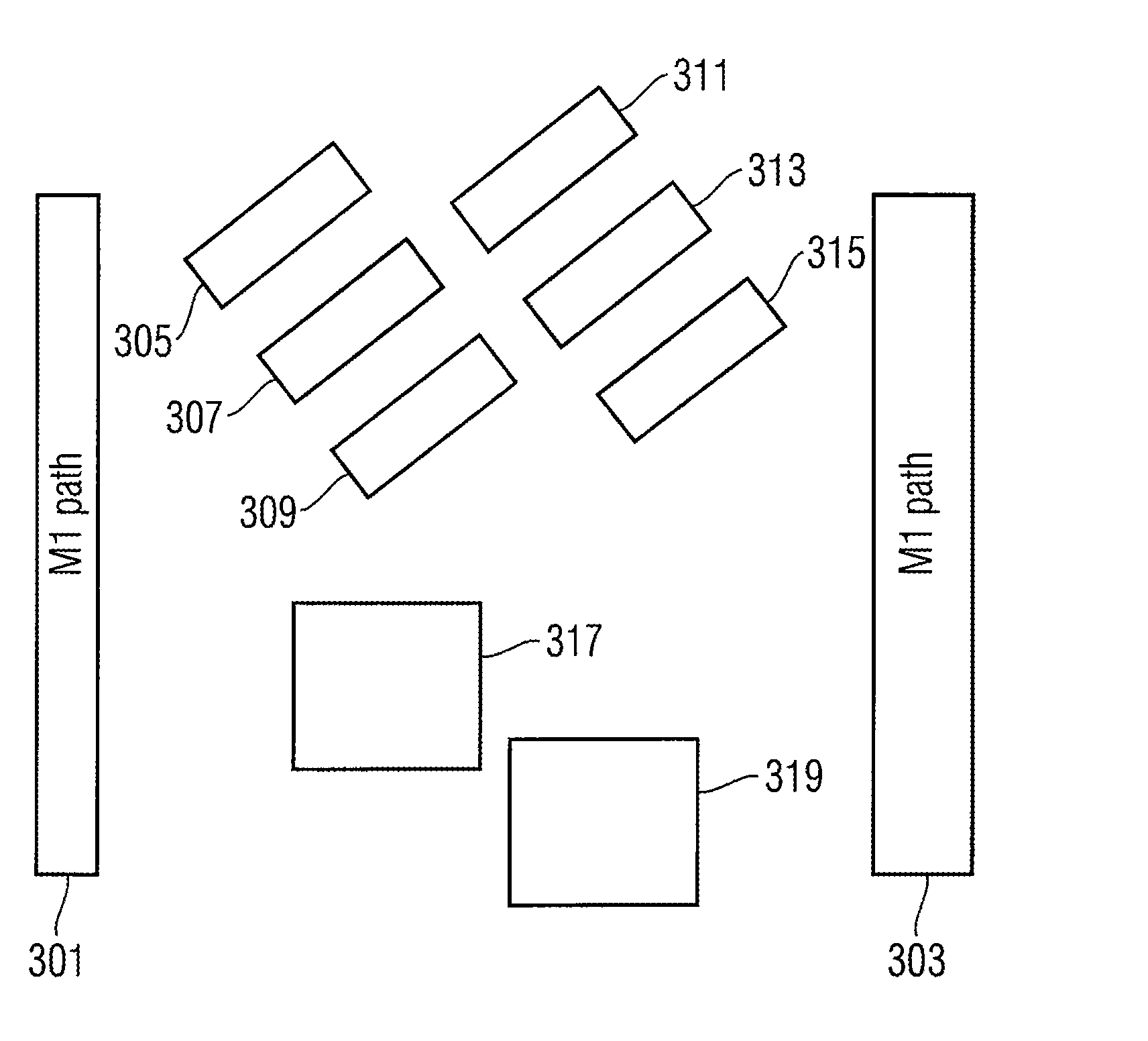
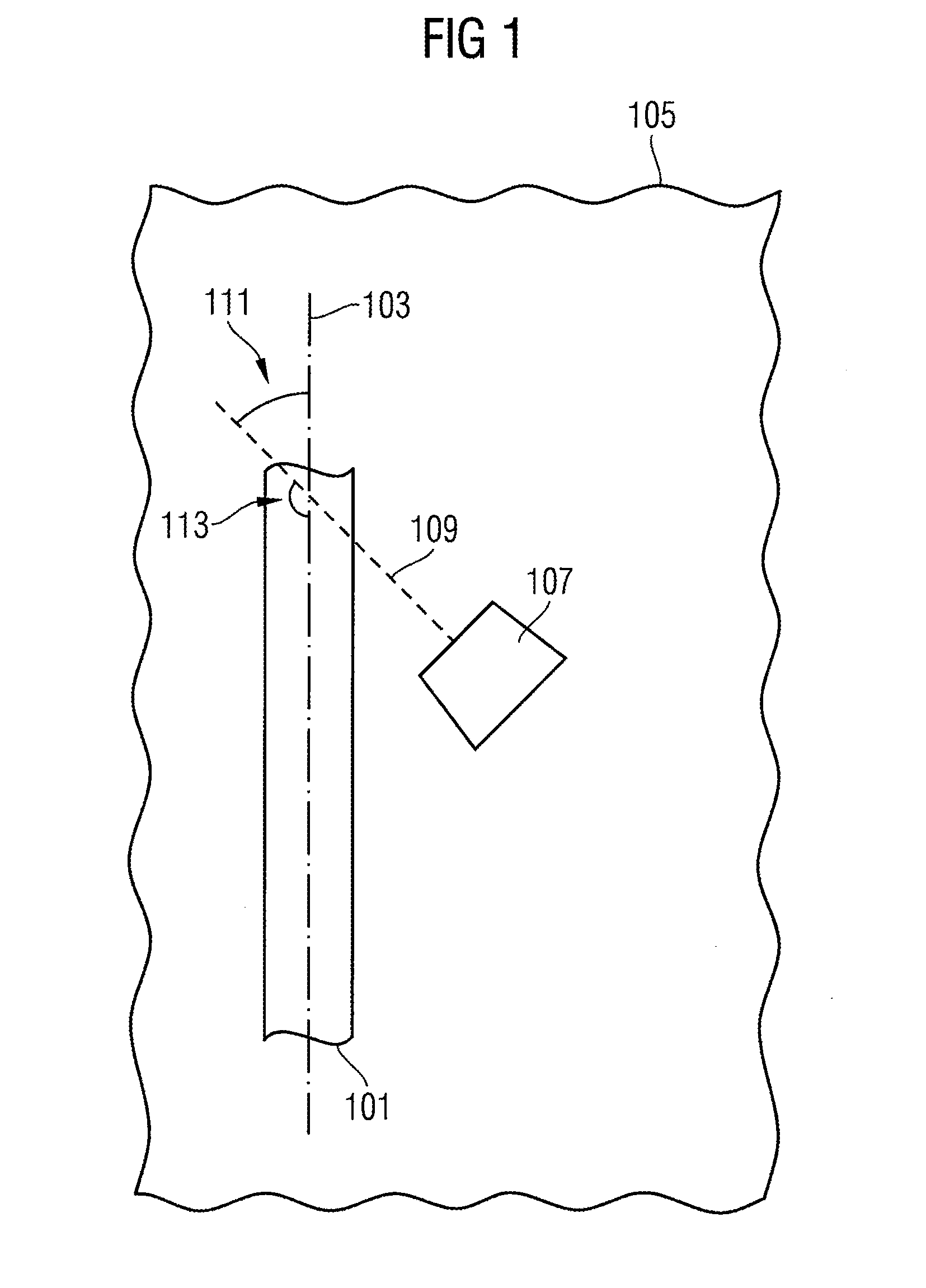
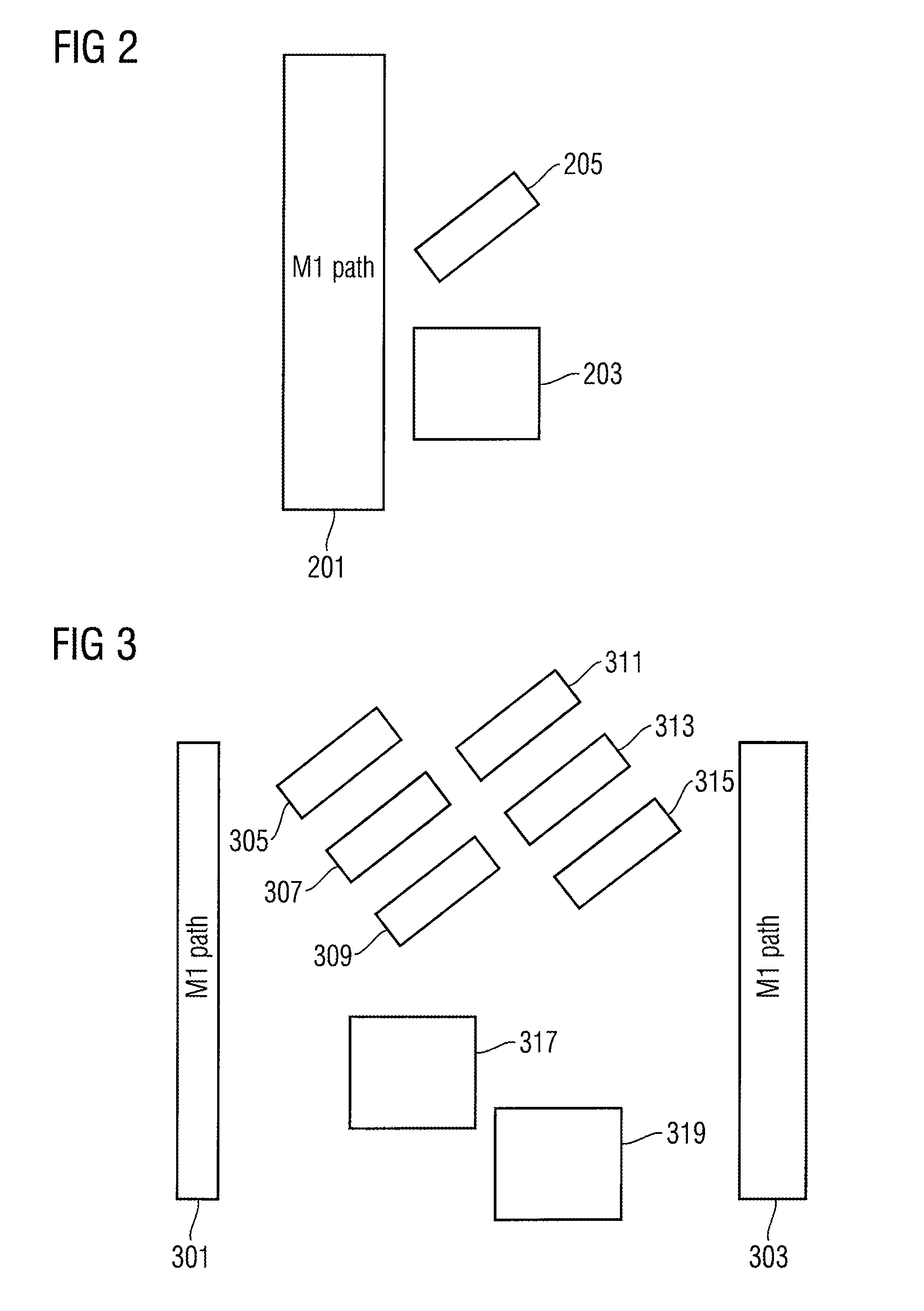
[0051]FIG. 1 shows a layout structure comprising a conducting line 101 extending in a conducting line direction 103. The conducting line 101 is arranged within a substrate area 105. The substrate area 105 may be arranged on a surface of or within the substrate, e.g. a silicon-based substrate. The layout structure further comprises a fill element 107 having a fill element axis 109 extending perpendicularly to a side of the fill element. In other words, the fill element axis 109 coincides with a fill element direction, wherein an angle 111 between the conducting line direction 103 and the fill element direction 109 is acute, i.e. greater than 0° and smaller than 90°. Correspondingly, a further angle 113 is greater than 90°. The fill element 107 has a substantially polygonal shape and, in a particular embodiment, is a parallelogram. For example, the fill element may have a substantially rectangular shape and is rotated relative to the conducting line by the angle 111. In the case of a ...


PUM


Abstract

A layout structure is provided with a conducting line extending in a conducting line direction, the conducting line being arranged within a substrate area, a fill element being arranged within the substrate area at a predetermined distance from the conducting line, the fill element having a fill element axis extending perpendicularly to a side of the fill element in a fill element direction, an angle between the conducting line direction and the fill element direction being greater than 0° and smaller than 90°.

Description

BACKGROUND OF THE INVENTION[0001]1. Field of the Invention[0002]The present invention is directed to a layout structure with a fill element arranged within a substrate area.[0003]2. Description of the Related Art[0004]In order to provide for a uniform metal density distribution across a chip or locally within a chip or substrate area, a fill pattern comprising fill elements influencing the coupling characteristic and further supporting the silicon processing with an impact on the yield and performance may be generated.[0005]Usually, fill elements are formed by conducting elements arranged e.g. in a vicinity of conducting lines. Unfortunately, a conductive fill pattern increases an interconnect (coupling) capacity which leads to an increased cross and noise coupling and therefore reduces the circuit performance and makes a timing sign-off difficult.[0006]In order to achieve a uniform density, smaller fill shapes filling smaller empty areas or a reduced distance of the fill pattern wi...

Claims


Application Information

Patent Timeline
IPC IPC(8): H01L27/10
CPCH01L23/49838H01L23/50H01L23/522H05K1/0216H01L2924/0002H05K2201/09781H01L2924/00
Inventor NIELSEN, ALEXANDERDOBLER, BERNHARDGEORGAKOS, GEORG
Owner INFINEON TECH AG
Features
  • Generate Ideas
  • Intellectual Property
  • Life Sciences
  • Materials
  • Tech Scout
  • Unparalleled Data Quality
  • Higher Quality Content
  • 60% Fewer Hallucinations
Learn More