Low-capacitance high-speed transmission semiconductor surge protection device

A surge protection device, high-speed transmission technology, used in semiconductor devices, electrical components, emergency protection circuit devices for limiting overcurrent/overvoltage, etc. The problem of strong avalanche current, etc., can improve the current density distribution, strong anti-surge ability and strong avalanche current resistance.

Inactive Publication Date: 2012-11-07
江苏锦丰电子有限公司
View PDF0 Cites 2 Cited by
  • Summary
  • Abstract
  • Description
  • Claims
  • Application Information

AI Technical Summary

Problems solved by technology

[0005] The purpose of the present invention is to solve the problem that the existing surge protection device will affect the transmission speed of the network when ensuring the safety of the equipment system, the efficiency is not high, and the problem that cannot meet the development requirements of the existing technology is proposed. + Balanced junction + SIPOS passivation" process produces low-capacity high-speed transmission semiconductor surge protection devices, which have the characteristics of small capacitance, strong anti-surge capability and strong avalanche current resistance, especially the small capacitance feature solves the problem of protection products for transmission information The key problem of attenuation, suitable for use in circuits with high data transmission speed

Method used


Image

  • Low-capacitance high-speed transmission semiconductor surge protection device

Examples


Embodiment Construction

[0019] The present invention will be further described below in conjunction with the accompanying drawings and embodiments.

[0020] A low-capacitance high-speed transmission semiconductor surge protection device, the PN junction is a flat PN junction balanced junction.

[0021] The emission zone of the semiconductor surge protection device of the present invention is injected twice.

[0022] P of the semiconductor surge protection device of the present invention - The thickness of the zone is deepened by 10%-20%.

[0023] N of the semiconductor surge protection device of the present invention - The thickness of the zone is thinned by 10-20%.

[0024] N of the present invention + The substrate is a double-sided polished silicon wafer with a thickness of 200-300 μm and a resistivity of 20-22%.

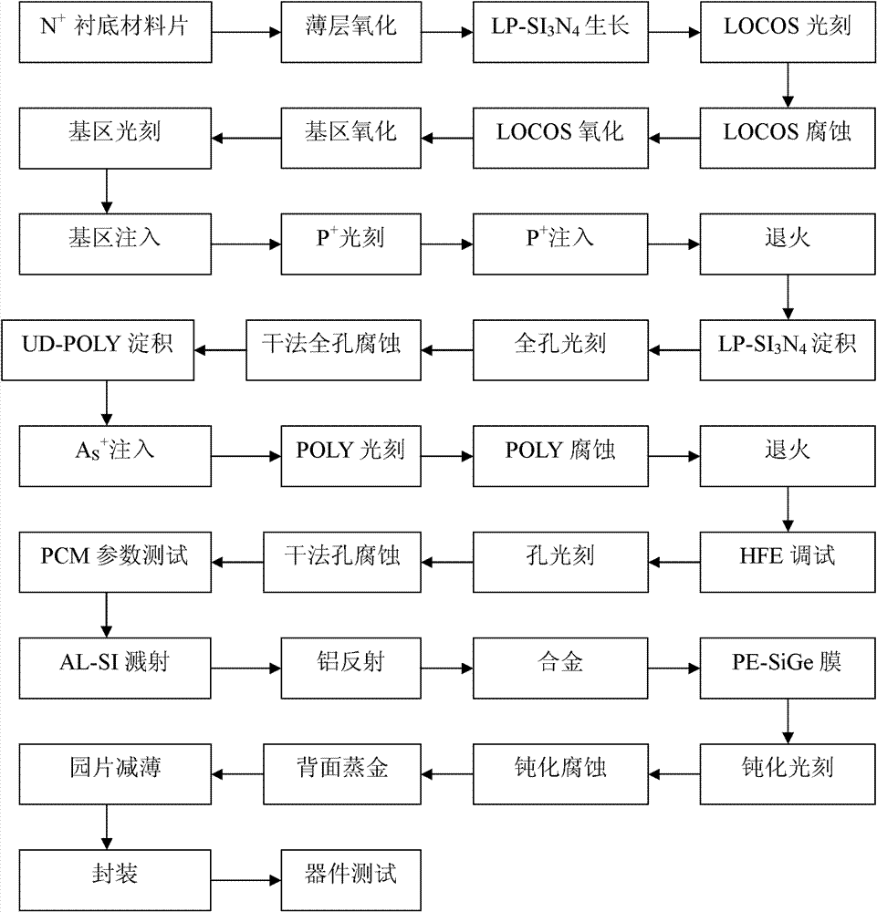
[0025] like figure 1 Shown is a schematic diagram of the technological process of the low-capacitance high-speed transmission semiconductor surge protection device of the present ...


PUM


Abstract

The invention discloses a low-capacitance high-speed transmission semiconductor surge protection device. The PN (P-type/N-type) junction is a flat PN junction equilibrium junction. Transmitting areas of the semiconductor surge protection device are filled for two times; the thickness of the P-area is increased by 10-20%; the thickness of the N-area is reduced by 10-20%; the N+substrate is a silicon wafer of which the two sides are polished; the thickness of the wafer ranges from 200-300 micrometers; and the resistivity is 20-22%. By adopting a flat PN junction equilibrium junction structure, the density distribution of the current is improved; by adopting the technology of increasing the thickness of the P-area, filling the transmitting area for two times, adopting a field plate and the like, a reverse breakdown voltage of a control tube EB (electron beam) is increased, and the contradiction between the reverse breakdown voltage of an EB junction and beta is solved; through the control to the beta of NPN (N-P-N type) of a quadruple structure thyristor, the problem of controlling the maintaining current and the breakover current is solved; and by decreasing the contact voltage and thinning the N-area, the minor carrier lifetime is increased.

Description

technical field [0001] The invention relates to a semiconductor surge protection device, in particular to a low-capacity high-speed transmission semiconductor surge protection device. Background technique [0002] Semiconductor overvoltage protection device is a new type of voltage suppressor. Because of its fast response speed, small size, stable performance, short-circuit protection and strong ability to absorb surge per unit area, it is widely used in anti-surge protection circuits of communication equipment. The working principle and basic structure of semiconductor overvoltage protection devices are similar to those of thyristors. Most of them use a four-layer PNPN structure at both ends. The avalanche breakdown of the PN junction or the gate current triggers the rapid conduction of the device, so that when a power surge occurs Play the role of voltage limiting protection for communication equipment. [0003] At present, the surge protection device (surge Protection D...

Claims


Application Information

Patent Timeline
Patent Type & Authority Applications(China)
IPC IPC(8): H01L29/06H01L29/74H02H9/04
Inventor 肖志良
Owner 江苏锦丰电子有限公司
Why Eureka
Try Eureka