

Ball grid array package structure
a package structure and grid array technology, applied in the field of semiconductor device package structure, can solve the problems of thin substrate depth, chip cracking of the package, damage to electronic devices, etc., and achieve the effect of reducing the warpage of the substrate, strengthening the bump, and improving the mechanical strength of the substrate of the ball grid array package structur
- Summary
- Abstract
- Description
- Claims
- Application Information
AI Technical Summary
Benefits of technology
Problems solved by technology
Method used
Image

Examples
Embodiment Construction
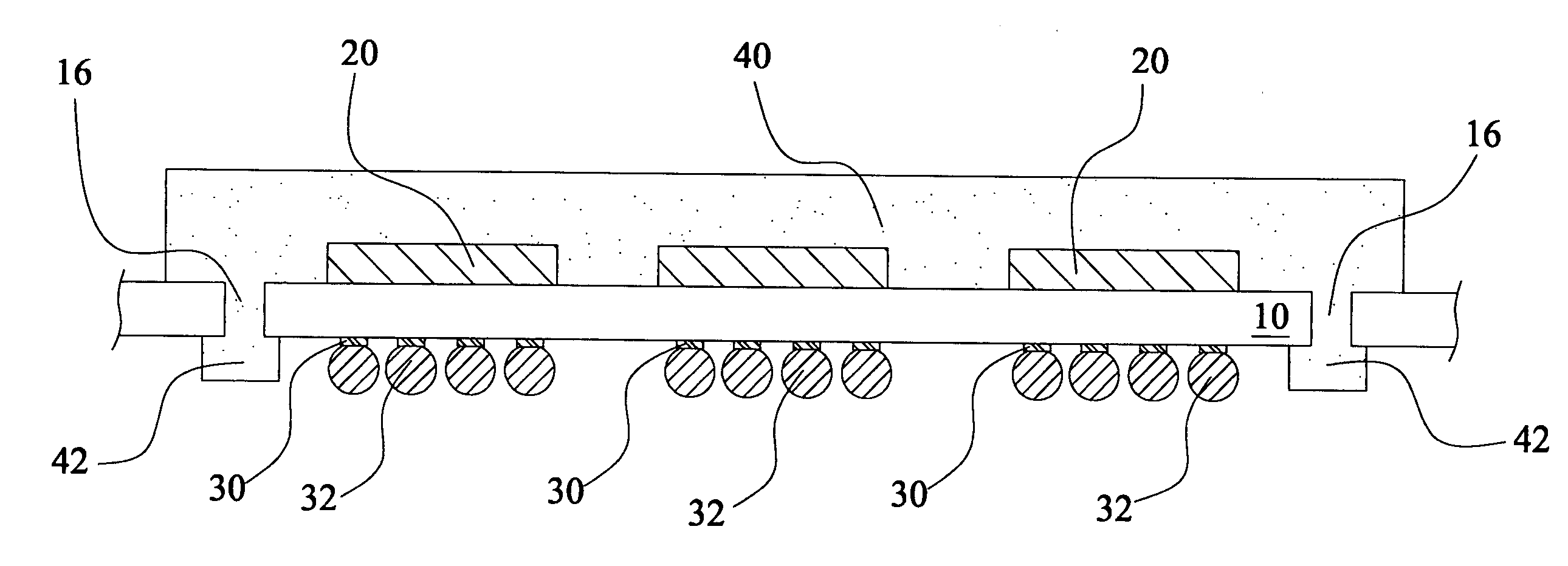
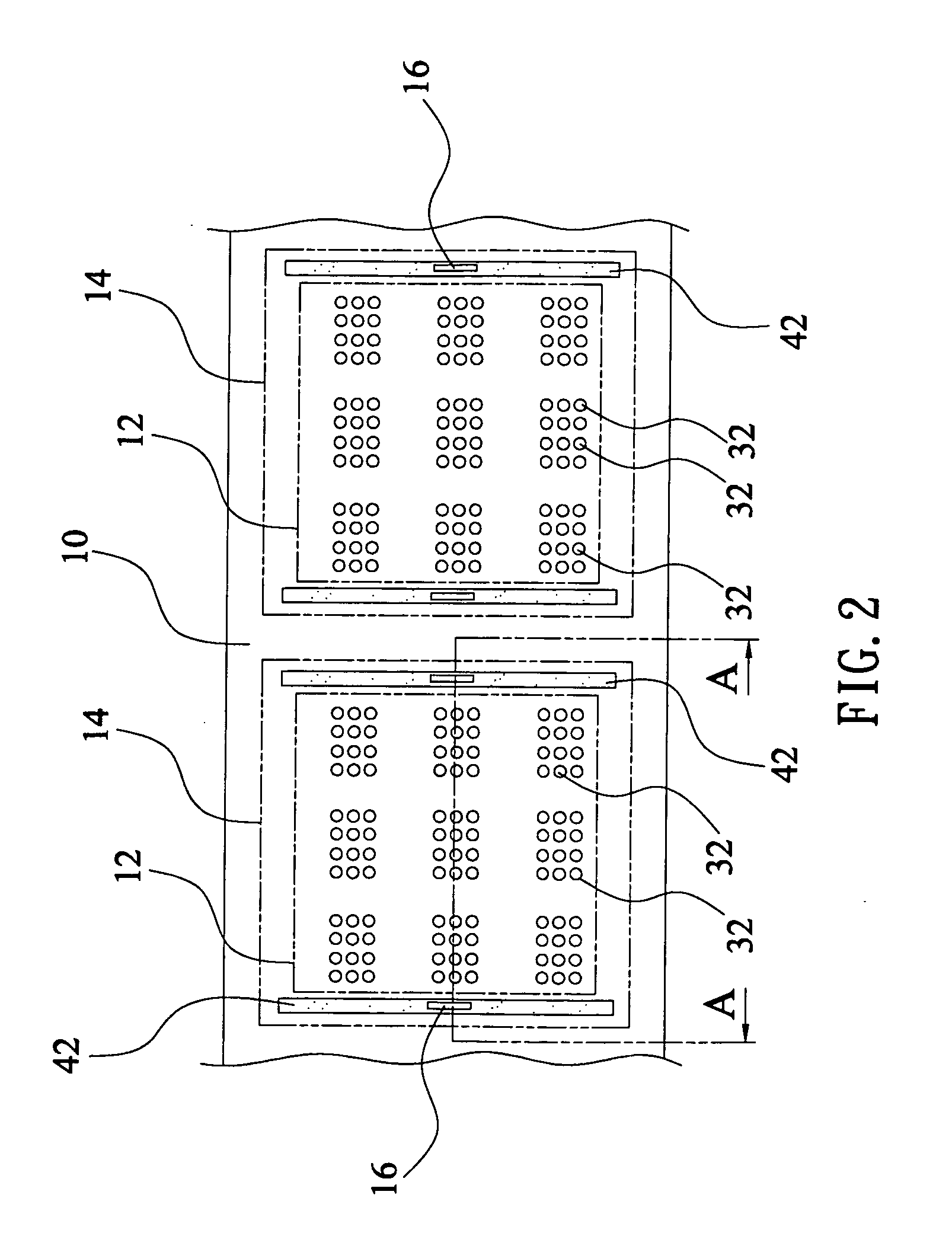
[0018]Please refer to FIG. 1, is a sectional diagram of the ball grid array package structure in accordance with an embodiment of the present invention. Shown in the figure, the BGA package structure includes a substrate 10, wherein the upper surface of the substrate 10 has at least one chip bearing area (not shown), and those electrical-connecting points 30 are arranged on the lower surface of the substrate 10; a plurality of chips 20 are arranged on the chip bearing area and electrically connected with those electrical-connecting points 30; a plurality of through holes 16 penetrate the substrate 10 at the edge of the chip bearing area; an encapsulant 40 used to cover those chips 20 and fills those through holes 16 to form a strengthened bump 42 surrounding the chip bearing area on the lower surface of the substrate 10; and a plurality of conductive balls 32 are respectively arranged on those electrical-connecting points 30.
[0019]In this embodiment, the substrate 10 is made of anyo...
PUM
 Abstract
Description
Claims
Application Information