Liquid crystal display

a technology of liquid crystal display and lcd panel, which is applied in the field of liquid crystal display, can solve the problems of increasing manufacturing cost, increasing the number of processes of lcd panel, and increasing the number of attached polarizers, so as to reduce the thickness reduce the cost and the number of processes. the effect of the lcd panel

Active Publication Date: 2008-05-01
SAMSUNG DISPLAY CO LTD
View PDF10 Cites 75 Cited by
  • Summary
  • Abstract
  • Description
  • Claims
  • Application Information

AI Technical Summary

Benefits of technology

[0014] According to one aspect of present invention a liquid crystal display (LCD) having a wire grid polarizer is formed when manufacturing the LCD panel, whereby the thickness of the LCD panel is reduced as compared with an attachable polarizer and the cost and the number of processes of the LCD panel can be reduced.

Problems solved by technology

While such a polarizer has a superior polarization characteristic, its manufacture requires an additional process besides those involved in manufacturing the LCD thereby increasing manufacturing cost.
Further, the existing attachable polarizer cannot provide polarization for each pixel of an LCD panel because the polarization characteristic are obtained by chemically bonding iodine molecules on the polyvinylalcohol (PVA) base film in a predetermined direction through wet stretching—resulting in the iodine molecules having a directional property throughout the entire film.
Thus, polarization cannot be individually provided for each pixel of an LCD.
Therefore, such a wire grid polarizer is more expensive than a film attachable polarizer in view of costs and the number of the entire processes.

Method used


Image

  • Liquid crystal display
  • Liquid crystal display
  • Liquid crystal display

Examples


first embodiment

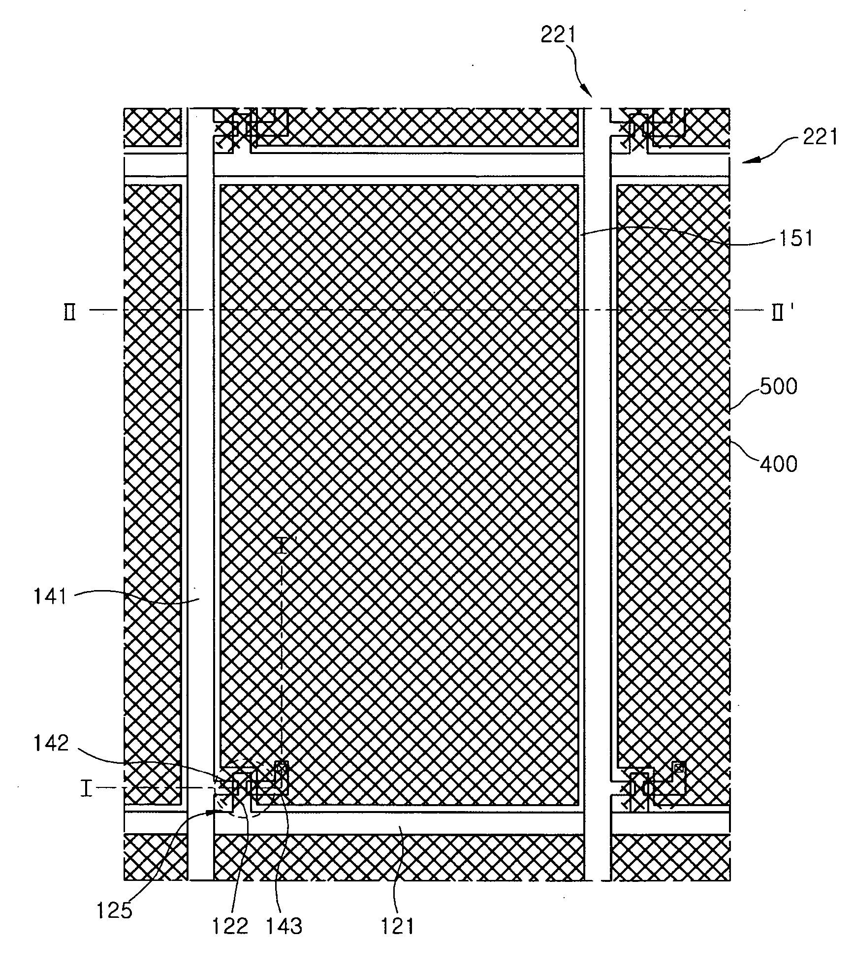
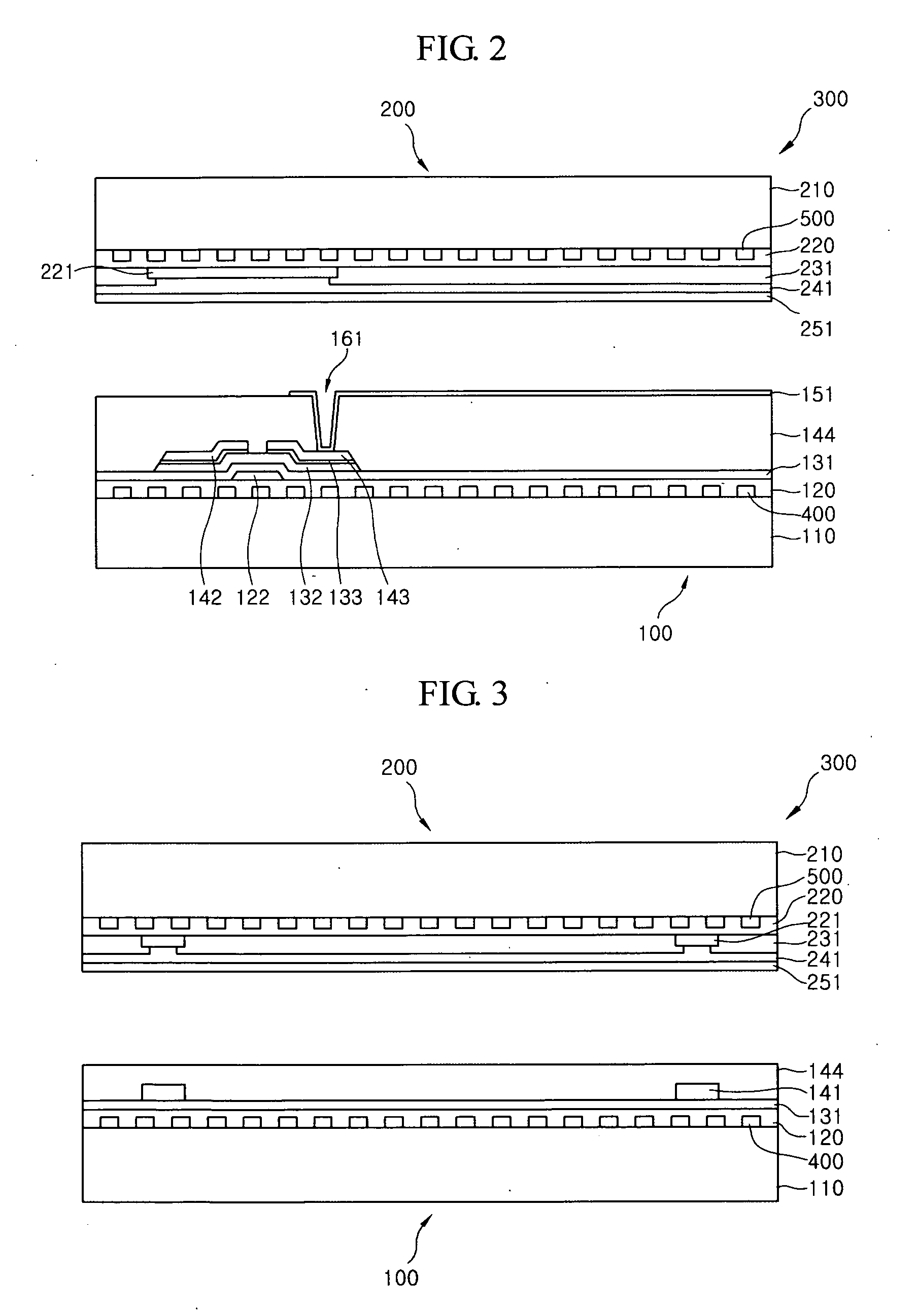
[0063]FIGS. 4A to 4F are sectional views sequentially illustrating a method of manufacturing a TFT substrate with a first wire grid polarizing pattern formed thereon according to the present invention.

[0064] Referring to FIG. 4A, a first conductive layer is formed on a substrate 110, and the first conductive layer is then patterned through a photo and etching process using a first mask to form a first wire grid polarizing pattern 400 with a predetermined line width and interval. Here, a metallic or non-metallic material including Al or other reflection materials is used to form the first conductive layer for the first wire grid polarizing pattern 400. Further, the first wire grid polarizing pattern 400 is formed on an entire surface of the substrate 110 to be aligned in one direction. For example, the first wire grid polarizing pattern 400 is formed in a direction parallel with or perpendicular to a gate line 121 or in an inclined direction at a predetermined angle with respect to t...

fourth embodiment

[0082]FIGS. 7A to 7C are sectional views sequentially illustrating a method of manufacturing a TFT substrate with a first wire grid polarizing pattern formed thereon according to the present invention, in which the first wire grid polarizing pattern is primarily formed on top of a substrate before a gate line is formed, and secondarily formed simultaneously with the gate line.

[0083] Referring to FIG. 7A, a first conductive layer is formed on top of a substrate 110 and then patterned through a photo and etching process using a predetermined mask so as to primarily form a first wire grid polarizing pattern 400a with a predetermined line width and interval. At this time, the interval between regions in which the primarily formed first wire grid polarizing pattern 400a is formed should be wider than a finally desired interval. For example, the interval between the regions in which the first wire grid polarizing pattern 400a is formed is twice or more than the finally desired interval. F...

fifth embodiment

[0086]FIGS. 8A to 8D are sectional views sequentially illustrating a method of manufacturing a TFT substrate with a first wire grid polarizing pattern formed thereon according to the present invention, in which the first wire grid polarizing pattern is primarily formed on top of a substrate before a gate line is formed, and secondarily formed simultaneously when a data line is formed.

[0087] Referring to FIG. 8A, a first conductive layer is formed on top of a substrate 110 and then patterned through a photo and etching process using a predetermined mask so as to primarily form a first wire grid polarizing pattern 400a with a predetermined line width and interval. At this time, the interval between regions in which the primarily formed first wire grid polarizing pattern 400a is formed should be formed wider twice or more than a finally desired interval. Further, an insulation film 120 is formed on top of the substrate 110 with the first wire grid polarizing pattern 400a primarily form...


PUM

PropertyMeasurementUnit
optical wavelengthaaaaaaaaaa
widthaaaaaaaaaa
widthaaaaaaaaaa

Abstract

The present invention relates to a liquid crystal display (LCD) and a method of manufacturing the same. In the present invention, a wire grid polarizing pattern is formed on at least one of thin film transistor and color filter substrates in a manufacturing process thereof. According to the present invention, the thickness of an LCD panel can be reduced as compared with a method of attaching an existing polarizer to an LCD panel, and the wire grid polarizing pattern can be built in an LCD panel without increasing the number of masking processes.

Description

REFERENCE TO RELATED APPLICATIONS [0001] This application claims the benefit of Korean patent application No. 10-2006-0104251 filed in the Korean Intellectual Property Office on Oct. 26, 2006 BACKGROUND OF THE INVENTION [0002] 1. Field of Invention [0003] The present invention relates to a liquid crystal display (LCD), and more particularly, to an LCD in which a wire grid polarizer is formed on at least one of a thin film transistor substrate and a color filter substrate. [0004] 2. Description of the Prior Art [0005] A liquid crystal display (LCD) comprises a thin film transistor (TFT) substrate with a pixel electrode formed thereon, a color filter substrate with a common electrode formed thereon, and a liquid crystal layer interposed between the two substrates. The LCD displays an image in such a manner that liquid crystal molecules are rearranged by applying a data voltage between the pixel and common electrodes to vary the amount of light transmitted through the liquid crystal la...

Claims


Application Information

Patent Timeline
Patent Type & Authority Applications(United States)
IPC IPC(8): G02F1/1335
CPCG02F1/133536G02F2001/133565G02F2001/133548G02F1/133548G02F1/133565G02F1/1335G02B5/30
Inventor CHOO, DAE HOAHN, YANG SUKYU, YEONG HEE
Owner SAMSUNG DISPLAY CO LTD
Why Eureka
Try Eureka