Plating Device, Plating Method, Semiconductor Device, And Method For Manufacturing Semiconductor Device

a technology of plating solution and semiconductor, which is applied in the manufacture of electrolysis components, tanks, manufacturing tools, etc., can solve the problems of oxidative decomposition of additives in the plating solution, deterioration of the quality of the plating solution, and consumption of more plating solution

Inactive Publication Date: 2008-05-08
SHARP KK
View PDF4 Cites 126 Cited by
  • Summary
  • Abstract
  • Description
  • Claims
  • Application Information

AI Technical Summary

Benefits of technology

[0022]The present invention was made in view of the foregoing problems. An object of the present invention is to provide: a plating device and a plating method each of which prevents minute solid foreign matters d...

Problems solved by technology

However, the conventional face-down type jet plating device has the following problem.
In the face-down type jet plating device, minute solid foreign matters attach to a surface-to-be-plated, resulting in deterioration in plating quality.
However, at that time, an additive in the pla...

Method used


Image

  • Plating Device, Plating Method, Semiconductor Device, And Method For Manufacturing Semiconductor Device
  • Plating Device, Plating Method, Semiconductor Device, And Method For Manufacturing Semiconductor Device
  • Plating Device, Plating Method, Semiconductor Device, And Method For Manufacturing Semiconductor Device

Examples


embodiment 1

[0058]With reference to FIGS. 1 to 6, the following explains an embodiment of the present invention.

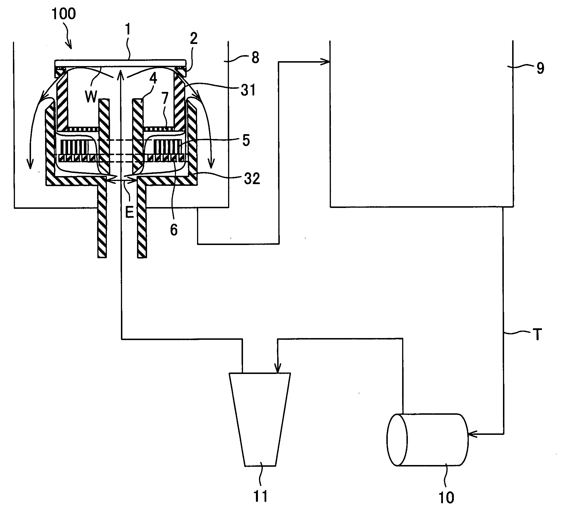
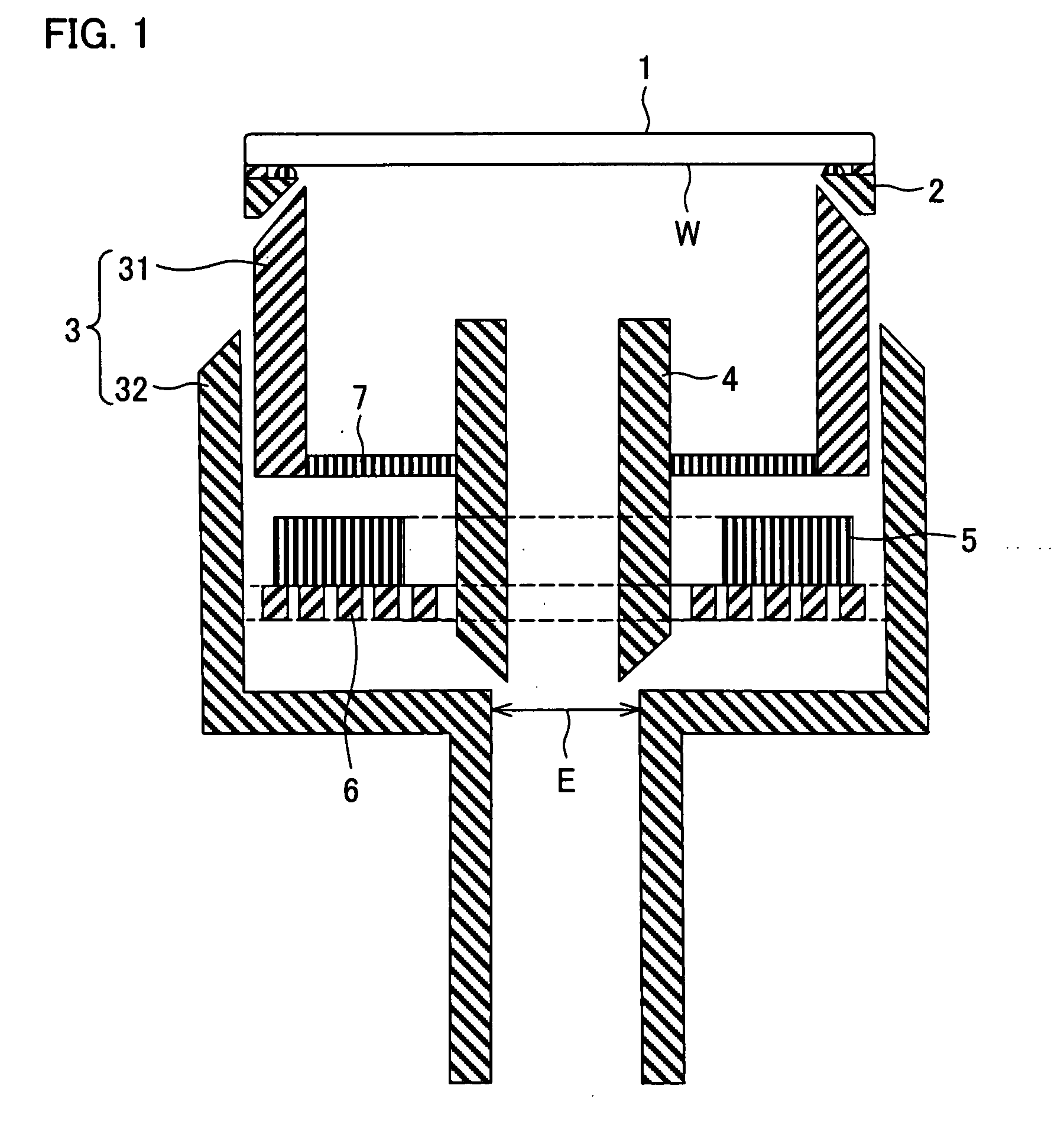
[0059]FIG. 1 is a cross sectional drawing schematically illustrating a structure of a plating tank provided in a plating device of the present embodiment. As shown in FIG. 1, a plating tank 100 includes: a wafer holder 2 for holding a semiconductor wafer (substrate-to-be-plated) 1; a cup 3; a plating solution jetting pipe 4; an anode 5; a supporter 6 for supporting the anode 5; and a partition 7. The cup 3 includes an internal cylinder 31 and an external cylinder 32.

[0060]The internal cylinder (second cylindrical cup) 31 and the external cylinder (first cylindrical cup) 32 are cups each having substantially a cylindrical shape, with its upper end open. The diameter of the internal cylinder 31 is smaller than the diameter of the external cylinder 32. The external cylinder 32 has at its lowest central part a plating solution flowing-in port E through which a plating solution flows in.

[0...

embodiment 2

[0125]With reference to FIGS. 9 to 12, the present embodiment will detail the semiconductor wafer 1 used as a substrate to be plated in Embodiment 1 and a method for manufacturing the substrate. They are examples of a semiconductor device and a method for manufacturing the semiconductor device. FIG. 9 is a drawing schematically illustrating a structure of the semiconductor wafer 1 used in the present embodiment. FIG. 10 is a drawing schematically illustrating a structure of a semiconductor chip 33 formed on the semiconductor wafer 1 after a plating step. FIG. 10(a) is a plan drawing. FIG. 10(b) is a cross sectional drawing.

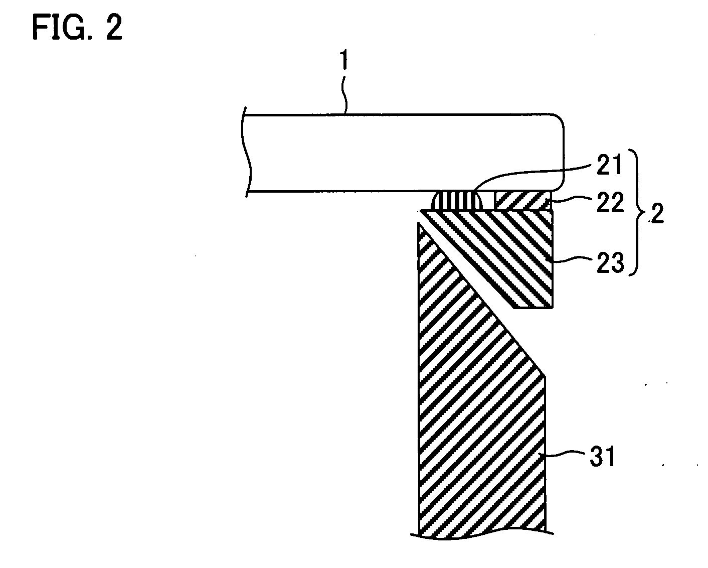
[0126]As illustrated in FIG. 9, a plurality of semiconductor chips 41 are formed on a surface of the semiconductor wafer 1. A contact section 42 is provided on the periphery of the semiconductor wafer 1. The contact section 42 includes a plating seed layer (not shown) which is exposed. The contact section 42 touches the contact member 22 illustrated in FIG. 2.

[012...


PUM

PropertyMeasurementUnit
Thicknessaaaaaaaaaa
Massaaaaaaaaaa
Flow rateaaaaaaaaaa

Abstract

An object of the present invention is to provide a face-down type jet plating device in which deterioration in plating quality due to minute solid foreign matters derived from a black film etc. is prevented without impairing operativity. The plating device is designed such that a partition (7) is provided between a semiconductor wafer (1) and an anode (5) so that the anode (5) and the semiconductor wafer (7) are separated from each other and a plating tank (100) is divided into a substrate-to-be-plated chamber and an anode chamber.

Description

TECHNICAL FIELD[0001]The present invention relates to a plating device, a plating method, a semiconductor device, and a method for manufacturing a semiconductor device. Specifically, the present invention relates to: a plating device and a plating method allowing minute plating for wiring to be formed on a surface to be plated; and a semiconductor device and a method for manufacturing the semiconductor deviceBACKGROUND ART[0002]Recently, metal plating is used for forming wiring on a semiconductor wafer and the like. Examples of a conventional device for metal plating include: a face-down type jet plating device; a rack-type vertical plating device; and a face-up type jet plating device.[0003]As shown in FIG. 7, the face-down type jet plating device includes: a wafer holder 2′ for holding a semiconductor wafer 1′; a cup 3′; a plating solution jetting pipe 4′ for supplying a plating solution into the cup 3′; and an anode 5′. The anode 5′ is generally made of high phosphorous copper. T...

Claims


Application Information

Patent Timeline
IPC IPC(8): C25D5/02C25D17/02C25D5/08C25D21/06
CPCC25D5/02C25D17/002C25D17/02C25D17/10C25D21/06H01L21/2885H01L24/11H01L2224/1148H01L2224/13099H01L2924/01011H01L2924/01015H01L2924/01022H01L2924/01027H01L2924/01029H01L2924/01074H01L2924/01075H01L2924/01078H01L2924/01079H01L2924/01082H01L2924/04953H01L2924/01005H01L2924/01006H01L2924/01019H01L2924/01024H01L2924/01033H01L2924/014C25D7/123C25D17/001C25D5/08H01L2224/05569H01L2224/05008H01L2224/05022H01L2224/05548H01L2224/05001H01L2224/05147H01L2224/05166H01L2224/05171H01L2224/05184H01L2224/05647H01L2224/13022H01L2224/13024H01L24/05H01L24/03H01L2224/0615H01L2224/023H01L2924/00014H01L2924/013H01L2924/0001
Inventor IWAZAKI, YOSHIHIDE
Owner SHARP KK
Why Eureka
Try Eureka