Front electrode including transparent conductive coating on patterned glass substrate for use in photovoltaic device and method of making same

a photovoltaic device and transparent conductive technology, applied in the field of front electrodes, can solve the problems of degrading the electrical properties of the tco front electrode of the photovoltaic device, increasing light input, and not significantly increasing the light path, so as to reduce visible light reflection, increase conductivity, and reduce the effect of visible light reflection

a photovoltaic device and transparent conductive technology, applied in the field of front electrodes, can solve the problems of degrading the electrical properties of the tco front electrode of the photovoltaic device, increasing light input, and not significantly increasing the light path, so as to reduce visible light reflection, increase conductivity, and reduce the effect of visible light reflection

US20080107799A1Inactive Publication Date: 2008-05-08GUARDIAN GLASS LLC

Image

  • Front electrode including transparent conductive coating on patterned glass substrate for use in photovoltaic device and method of making same
  • Front electrode including transparent conductive coating on patterned glass substrate for use in photovoltaic device and method of making same
  • Front electrode including transparent conductive coating on patterned glass substrate for use in photovoltaic device and method of making same

Examples


examples

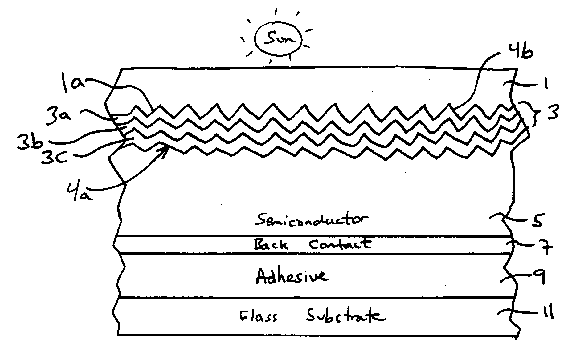
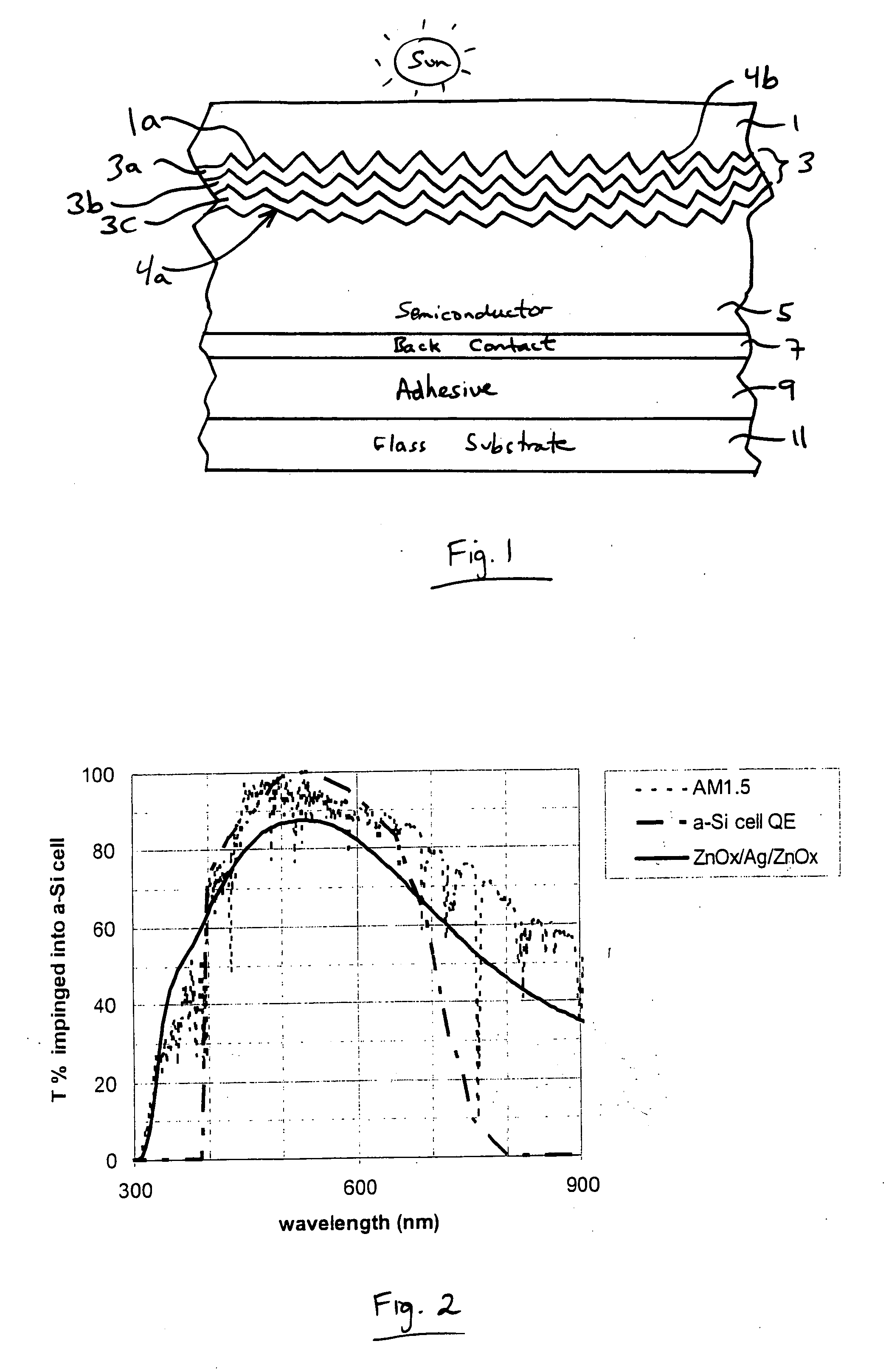
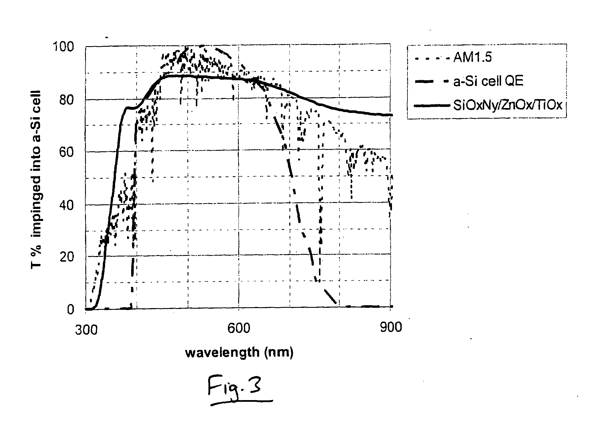
[0036]With reference to FIGS. 2-4 below, it will be explained how in certain example embodiments of this invention a single or multi-layered front electrode 3 can be designed in such a way that the maximum transmission is tailored to the quantum efficiency (QE) of the intended photovoltaic device and the light source spectrum. Then, this front electrode can be fabricated using a magnetron sputtering technique on pre-etched or pre-patterned glass 1. Due to the conformal characteristics of magnetron sputtering, multiple or single layered optical coatings for electrode 3 can be fabricated while preserving or substantially preserving the textured shape 1a of the substrate 1 in the major surface 4a of the electrode closest to the semiconductor film 5. In this way, the device output can be optimized through both improved light transmission and increased light path. The examples below each had more than 80% transmission (or at least 85%) into the semiconductor film 5 in part or all of the ...


PUM

PropertyMeasurementUnit
wavelength rangeaaaaaaaaaa
IR wavelengthaaaaaaaaaa

Abstract

This invention relates to a photovoltaic device including an electrode such as a front electrode / contact. In certain example embodiments, the front electrode of the photovoltaic device includes a multi-layered transparent conductive coating which is sputter-deposited on a textured surface of a patterned glass substrate. In certain example embodiments, a maximum transmission area of the substantially transparent conductive front electrode is located under a peak area of a quantum efficiency (QE) curve of the photovoltaic device and a light source spectrum used to power the photovoltaic device.

Description

[0001]This application is a continuation-in-part (CIP) of U.S. Ser. No. 11 / 591,668, filed Nov. 2, 2006, the entire disclosure of which is hereby incorporated herein by reference.[0002]This invention relates to a photovoltaic device including an electrode such as a front electrode / contact. In certain example embodiments, the front electrode of the photovoltaic device includes a conformal transparent conductive coating (single or multi-layered) which is sputter-deposited on a textured surface of a patterned glass substrate. In certain example instances, this is advantageous in that efficiency of the photovoltaic device can be improved by increasing light absorption by the active semiconductor via both increasing light intensity passing through the front glass substrate and front electrode, and increasing the light path in the semiconductor photovoltaic conversion layer.BACKGROUND AND SUMMARY OF EXAMPLE EMBODIMENTS OF INVENTION[0003]Photovoltaic devices are known in the art (e.g., see ...

Claims


Application Information

Patent Timeline
08 May 2008
Publication
US20080107799A1
IPC
B05D5/12
CPC
H01L31/022425; H01L31/022466; H01L31/0236; Y02E10/548; H01L31/075; H01L31/1884; H01L31/048; H01L31/0488
Inventors
LU, YIWEI; DEN BOER, WILLEM