
Back reflector for use in photovoltaic device

Inactive Publication Date: 2008-09-18
GUARDIAN GLASS LLC
View PDF16 Cites 166 Cited by
  • Summary
  • Abstract
  • Description
  • Claims
  • Application Information

AI Technical Summary

Benefits of technology

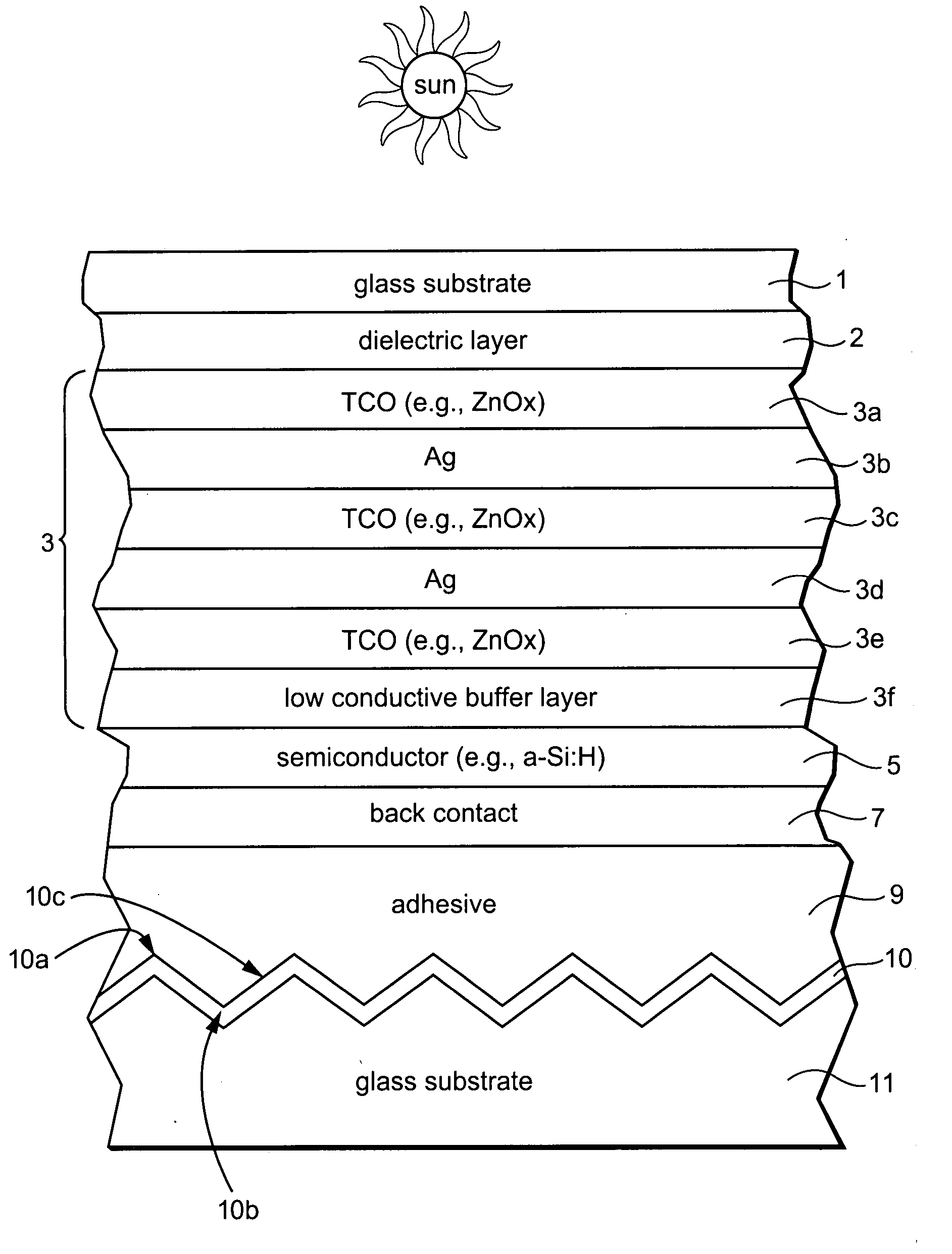
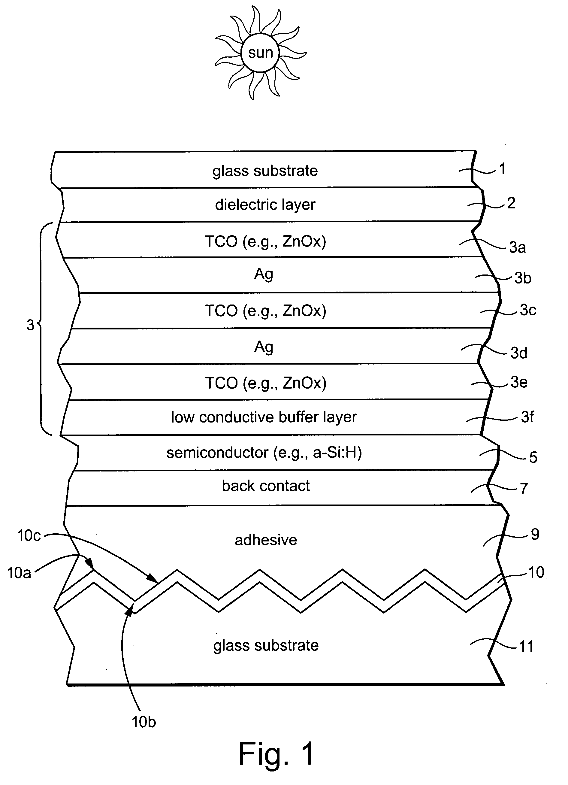
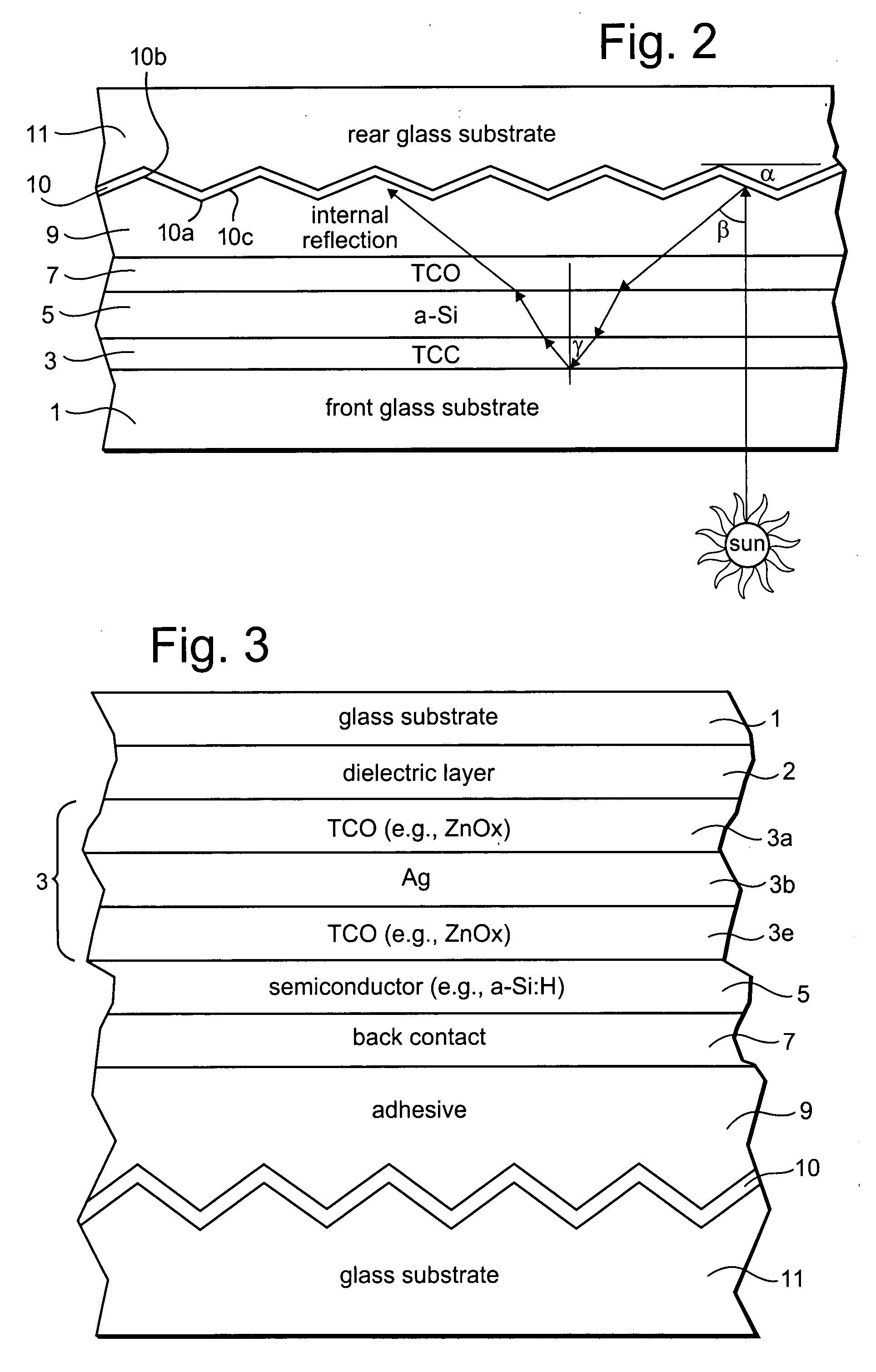
[0008]In certain example embodiments of this invention, optionally, the front electrode of the photovoltaic device may be comprised of a multilayer coating including at least one transparent conductive oxide (TCO) layer (e.g., of or including a material such as tin oxide, zinc oxide, or the like) and at least one conductive substantially metallic IR reflecting layer (e.g., based on silver, gold, or the like). In certain example instances, the multilayer front electrode coating may include a plurality of TCO layers and/or a plurality of conductive substantially metallic IR reflecting layers arranged in an alternating manner in order to provide for reduced visible light reflections, increased conductivity, increased IR reflection capability, and so forth. In certain example embodiments of this invention, such a multilayer front electrode coating may be flat and be designed to realize one or more of the following advantageous features: (a) reduced sheet resistance (R,) and thus increased conductivity and imp

Problems solved by technology

Unfortunately, photovoltaic devices (e.g., solar cells) such as that discussed above suffer from one or more of the following problems.
Second, there may be an impact on reliability of the semiconductor (e.g., a-Si) when it follows the texture of the front electrode, potentially leading to shorts, weak points, and / or other defects in the semiconductor film—in particular when it is very thin.
Third, the materials from which the front electrode are made may be limited as certain alternative types of front electrode materials tend to realize an increase in resistance when they are textured and not smooth.
Fourth, the front electrode TCO needs to be relatively thick (e.g., 400-800 nm) to obtain acceptable sheet resistance, thereby increasing costs and lowering manufacturing throughput.

Method used


Image

  • Back reflector for use in photovoltaic device
  • Back reflector for use in photovoltaic device
  • Back reflector for use in photovoltaic device

Examples


Embodiment Construction

[0019]Referring now more particularly to the figures in which like reference numerals refer to like parts / layers in the several views.

[0020]Photovoltaic devices such as solar cells convert solar radiation into usable electrical energy. The energy conversion occurs typically as the result of the photovoltaic effect. Solar radiation (e.g., sunlight) impinging on a photovoltaic device and absorbed by an active region of semiconductor material (e.g., a semiconductor film including one or more semiconductor layers such as a-Si layers, the semiconductor sometimes being called an absorbing layer or film) generates electron-hole pairs in the active region. The electrons and holes may be separated by an electric field of a junction in the photovoltaic device. The separation of the electrons and holes by the junction results in the generation of an electric current and voltage. In certain example embodiments, the electrons flow toward the region of the semiconductor material having n-type con...


PUM


Abstract

This invention relates to a photovoltaic device including a back reflector. In certain example embodiments, the back reflector includes a metallic based reflective layer provided on an interior surface of a rear glass substrate of the photovoltaic device. In certain example embodiments, the interior surface of the rear glass substrate is textured so that the reflector layer deposited thereon is also textured so as to provide desirable reflective characteristics. The rear glass substrate and reflector thereon are laminated to the interior surface of a front glass substrate of the photovoltaic device, with an active semiconductor film and electrode(s) therebetween, in certain example embodiments.

Description

[0001]This invention relates to a photovoltaic device including a back reflector. In certain example embodiments of this invention, the back reflector includes a metallic based reflective layer provided on an interior surface of a rear glass substrate of the photovoltaic device. In certain example embodiments, the interior surface of the rear glass substrate is textured so that the reflector layer deposited thereon is also textured so as to provide desirable reflective characteristics. The rear glass substrate and reflector thereon are laminated to the interior surface of a front glass substrate of the photovoltaic device, with an active semiconductor film and electrode(s) therebetween, in certain example embodiments.BACKGROUND AND SUMMARY OF EXAMPLE EMBODIMENTS OF INVENTION[0002]Photovoltaic devices are known in the art (e.g., see U.S. Pat. Nos. 6,784,361, 6,288,325, 6,613,603, and 6,123,824, the disclosures of which are hereby incorporated herein by reference). Amorphous silicon (...

Claims


Application Information

Patent Timeline
IPC IPC(8): H01L31/0216
CPCH01L31/022466H01L31/0236H01L31/056H01L31/02167H01L31/048Y02E10/52H01L31/022483H01L31/02366H01L31/0488H01L31/0445
Inventor DEN BOER, WILLEMLU, YIWEI
Owner GUARDIAN GLASS LLC
Learn More