Fabricating non-volatile memory with boost structures

a non-volatile memory and boost technology, applied in the field of non-volatile memory, can solve problems such as program disturban

Active Publication Date: 2008-05-15
SANDISK TECH LLC
View PDF42 Cites 19 Cited by
  • Summary
  • Abstract
  • Description
  • Claims
  • Application Information

AI Technical Summary

Benefits of technology

[0018]In another embodiment, a method for fabricating non-volatile storage includes forming a number of NAND strings on a substrate, forming a number of boost structures, each boost structure extending a

Problems solved by technology

However, during programming, various problems such as program disturb can

Method used


Image

  • Fabricating non-volatile memory with boost structures
  • Fabricating non-volatile memory with boost structures
  • Fabricating non-volatile memory with boost structures

Examples


Embodiment Construction

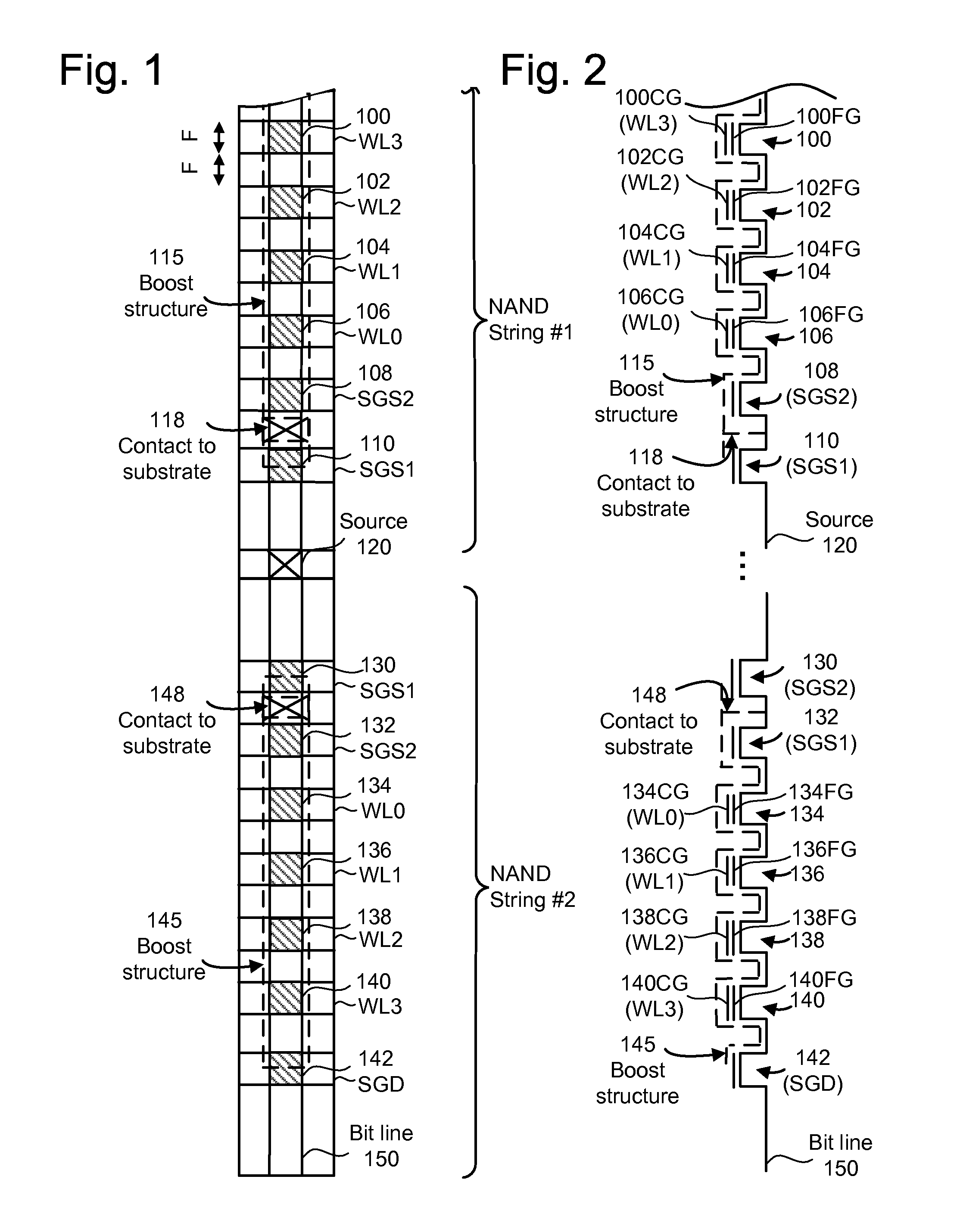
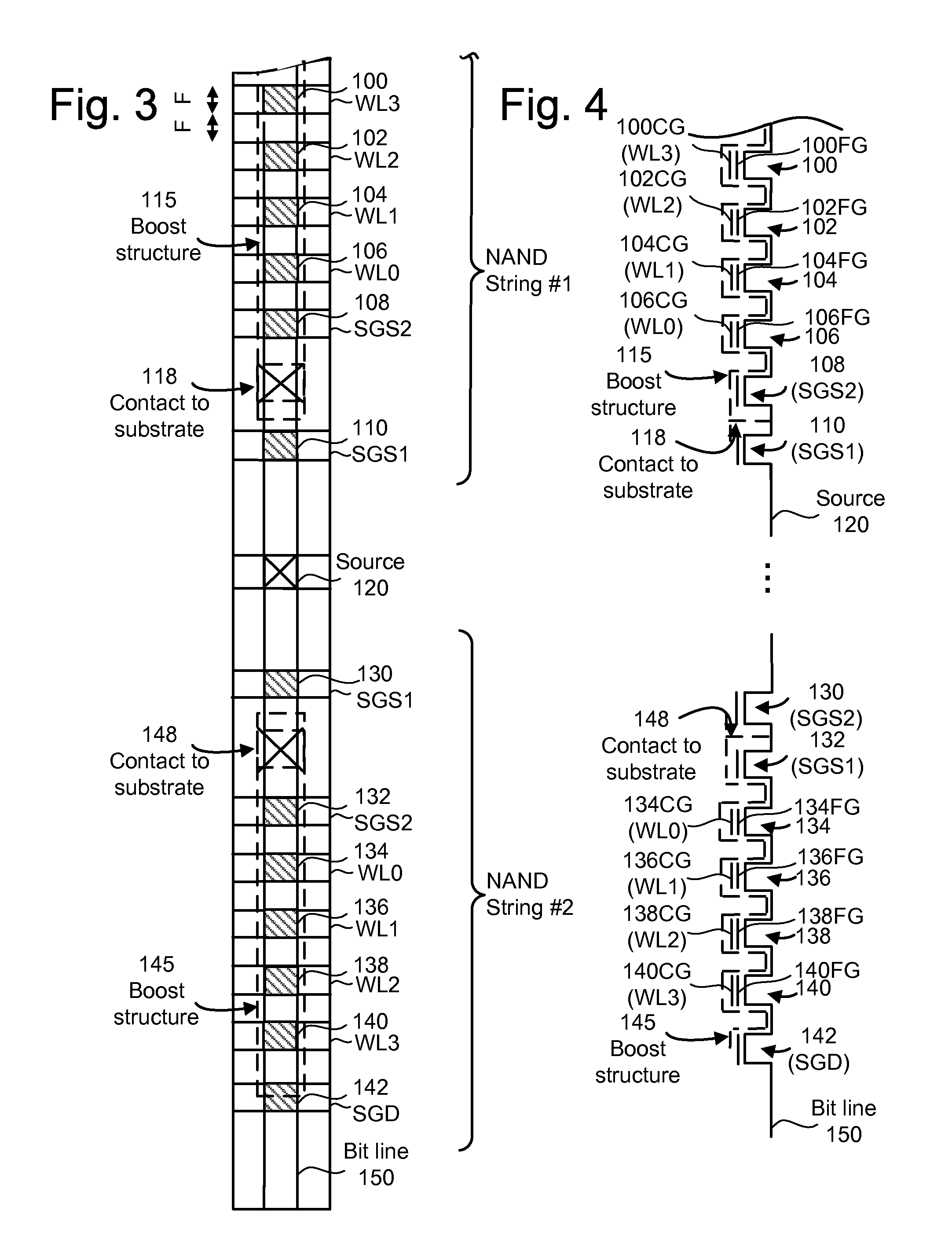
[0051]One example of a non-volatile memory system suitable for use with the present invention uses a NAND flash memory structure, in which multiple transistors are arranged in series between select gates in a NAND string. FIG. 1 is a top view showing two NAND strings arranged one after another. In practice, a number of such NAND strings can be arranged one after another in a two-dimensional array across a semiconductor device and, optionally, in three dimensions. The NAND strings depicted in FIGS. 1 and 2 each include four transistors in series and sandwiched between select gates. In one embodiment, each NAND string includes two source-side select gates and one drain-side select gate. For example NAND string #1 includes transistors 100, 102, 104 and 106 sandwiched between a drain-side select gate (not shown) and source-side select gates 108 and 110. Select gates 108 and 110 can be connected to, or provided as part of, control lines SGS2 and SGS1, respectively, of the associated NAND...


PUM


Abstract

A method for fabricating a non-volatile memory having boost structures. Boost structures are provided for individual NAND strings and can be individually controlled to assist in programming, verifying and reading processes. The boost structures can be commonly boosted and individually discharged, in part, based on a target programming state or verify level. The boost structures assists in programming so that the programming and pass voltage on a word line can be reduced, thereby reducing side effects such as program disturb. During verifying, all storage elements on a word line can be verified concurrently. The boost structure can also assist during reading. In one approach, the NAND string has dual source-side select gates between which the boost structure contacts the substrate at a source/drain region, and a boost voltage is provided to the boost structure via a source-side of the NAND string.

Description

CROSS-REFERENCE TO RELATED APPLICATIONS [0001]This application is related to co-pending, commonly assigned U.S. patent application Ser. No. ______, filed ______, titled “Operating Non-Volatile Memory With Boost Structures” (docket no. SAND-1126US0), and co-pending, commonly assigned U.S. patent application Ser. No. ______, filed ______, titled “Non-Volatile Memory With Boost Structures” (docket no. SAND-1126US1), each of which is incorporated herein by reference.BACKGROUND OF THE INVENTION[0002]1. Field of the Invention[0003]The present invention relates to non-volatile memory.[0004]2. Description of the Related Art[0005]Semiconductor memory has become increasingly popular for use in various electronic devices. For example, non-volatile semiconductor memory is used in cellular telephones, digital cameras, personal digital assistants, mobile computing devices, non-mobile computing devices and other devices. Electrically Erasable Programmable Read Only Memory (EEPROM) and flash memory...

Claims


Application Information

Patent Timeline
IPC IPC(8): H01L21/8247
CPCG11C11/5628G11C16/0483G11C16/10H01L27/11524G11C16/3427H01L27/115H01L27/11521G11C16/3418H10B41/35H10B69/00H10B41/30
Inventor MOKHLESI, NIMA
Owner SANDISK TECH LLC
Why Eureka
Try Eureka