

Method of fabricating a nitride semiconductor light emitting device
a technology of nitride and light-emitting devices, which is applied in the manufacture of semiconductor/solid-state devices, semiconductor devices, electrical equipment, etc., can solve the problems of reduced transmittance for visible light, limited temperature range in the process after the formation of impaired transparent conductive films of ito. , to achieve the effect of increasing the energy gap between tunnel junctions, reducing the probability of tunneling, and increasing the loss of voltag
- Summary
- Abstract
- Description
- Claims
- Application Information
AI Technical Summary
Benefits of technology
Problems solved by technology
Method used
Image

Examples
first example
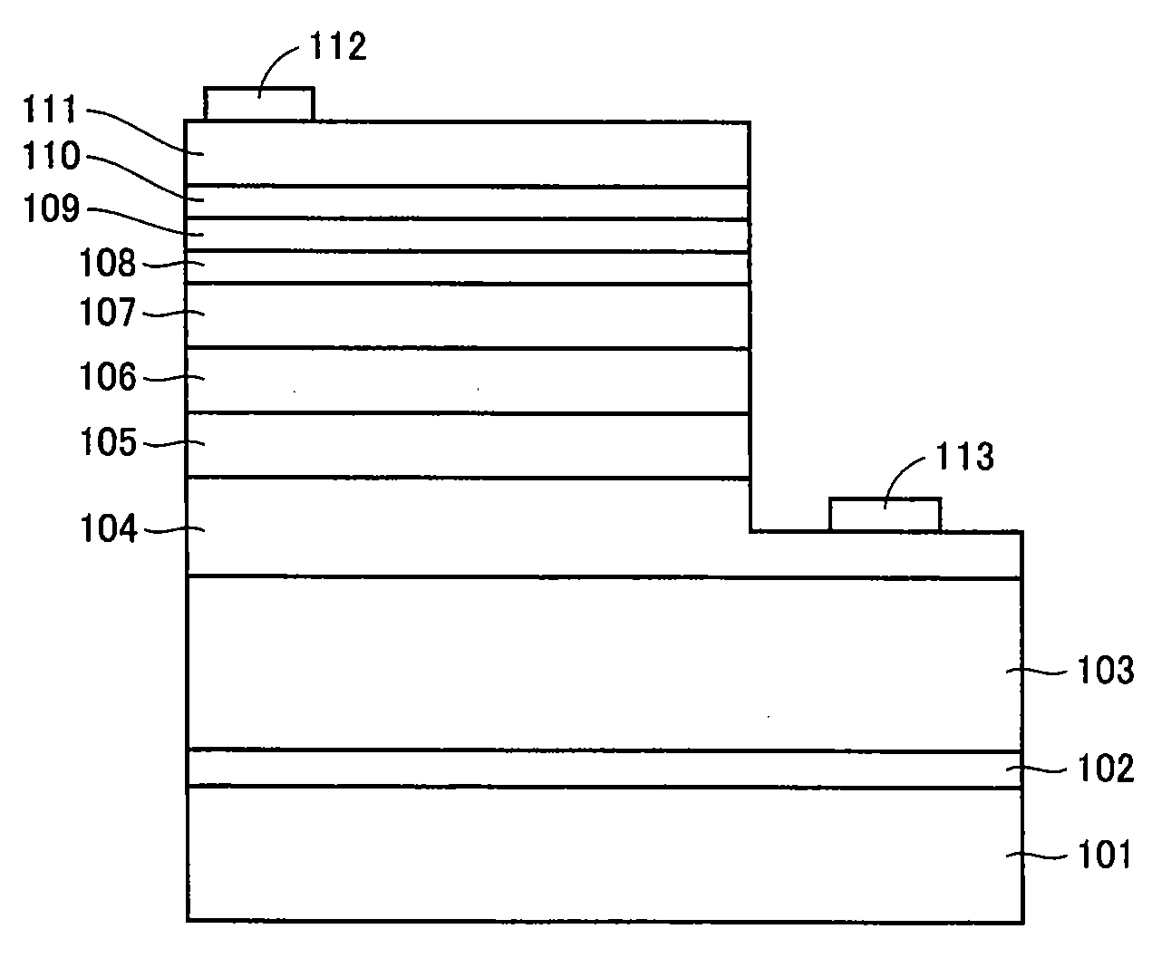
[0067]The first example provides the nitride semiconductor light emitting diode device configured as shown in FIG. 11. The first example's nitride semiconductor light emitting diode device includes, a GaN buffer layer 102, an n-type GaN underlying layer 103, an n-type GaN contact layer 104, a light emitting layer 105, a p-type AlGaN clad layer 106, a p-type GaN layer 107, a p-type InGaN tunnel junction layer 108, an n-type InGaN tunnel junction layer 109, an n-type GaN evaporation reduction layer 110, and an n-type GaN layer 111, deposited on a sapphire substrate 101 in this order and a pad electrode 112 deposited on a surface of n-type GaN layer 111 and a pad electrode 113 deposited on a surface of n-type GaN contact layer 104.
[0068]Initially sapphire substrate 101 is set in a reactor of an MOCVD apparatus. Subsequently hydrogen is flown into the reactor, while the temperature of sapphire substrate 101 is increased to 1050° C. to clean a surface (a C plane) of sapphire substrate 10...
second example
[0085]Up to growing n-type InGaN tunnel junction layer 109, the temperature of the same conditions and method as the first example are applied.
[0086]After n-type InGaN tunnel junction layer 109 is grown, the temperature of sapphire substrate 101 is held at 700° C. and only TMI is stopped to grow n-type GaN evaporation reduction layer 110 formed of GaN doped with Si at a concentration of 1×10²⁰ atoms / cm3, by MOCVD to have a thickness of 15 nm on n-type InGaN tunnel junction layer 109.
[0087]Subsequently the temperature of sapphire substrate 101 is set at a predetermined temperature between 700° C. and 1050° C. and a carrier gas of hydrogen, source material gases of ammonium and TMG, and an impurity gas of silane are flown into the reactor to grow n-type GaN layer 111 formed of GaN doped with Si at a concentration of 1×10¹⁹ atoms / cm3, by MOCVD to have a thickness of 200 nm on n-type GaN evaporation reduction layer 110.
[0088]Subsequently the same conditions and method as the first examp...
third example
[0095]Up to growing p-type InGaN tunnel junction layer 108, the same conditions and method as the first example are applied.
[0096]After p-type InGaN tunnel junction layer 108 is grown, the temperature of sapphire substrate 101 is held at 700° C. and only TMI is stopped to grow n-type GaN evaporation reduction layer 110 formed of GaN doped with Si at a concentration of 1×10²⁰ atoms / cm3, by MOCVD to have a thickness of 0 nm to 15 nm on p-type InGaN tunnel junction layer 108.
[0097]Subsequently the same conditions and method as the first example are applied to fabricate a nitride semiconductor light emitting diode device of the third example.
[0098]FIG. 15 shows a relationship between the thickness of n-type GaN evaporation reduction layer 110 of the nitride semiconductor light emitting diode device of the third example and the driving voltage of the device. In FIG. 15, the vertical axis represents the driving voltage (V) at the time when a current of 20 mA is injected, and the horizonta...
PUM
| Property | Measurement | Unit |
|---|---|---|
| temperature | aaaaa | aaaaa |
| temperature | aaaaa | aaaaa |
| temperature | aaaaa | aaaaa |
Abstract
Description
Claims
Application Information