Method of making a strained semiconductor device

Inactive Publication Date: 2008-05-22
IBM CORP +1
View PDF4 Cites 31 Cited by
  • Summary
  • Abstract
  • Description
  • Claims
  • Application Information

AI Technical Summary

Problems solved by technology

One other challenge is to increase the mobility of semiconductor carriers such as electrons and holes.
Since the germanium crystal lattice is larger than silicon, the germanium-containing layer creates a lattice mismatch stress in adjacent layers.

Method used


Image

  • Method of making a strained semiconductor device
  • Method of making a strained semiconductor device
  • Method of making a strained semiconductor device

Examples


Embodiment Construction

[0014]The making and using of the presently preferred embodiments are discussed in detail below. It should be appreciated, however, that the present invention provides many applicable inventive concepts that can be embodied in a wide variety of specific contexts. The specific embodiments discussed are merely illustrative of specific ways to make and use the invention, and do not limit the scope of the invention.

[0015]The invention will now be described with respect to preferred embodiments in a specific context, namely a method for improving carrier mobility in a CMOS device. Concepts of the invention can also be applied, however, to other electronic devices. As but one example, bipolar transistors (or BiCMOS) can utilize concepts of the present invention.

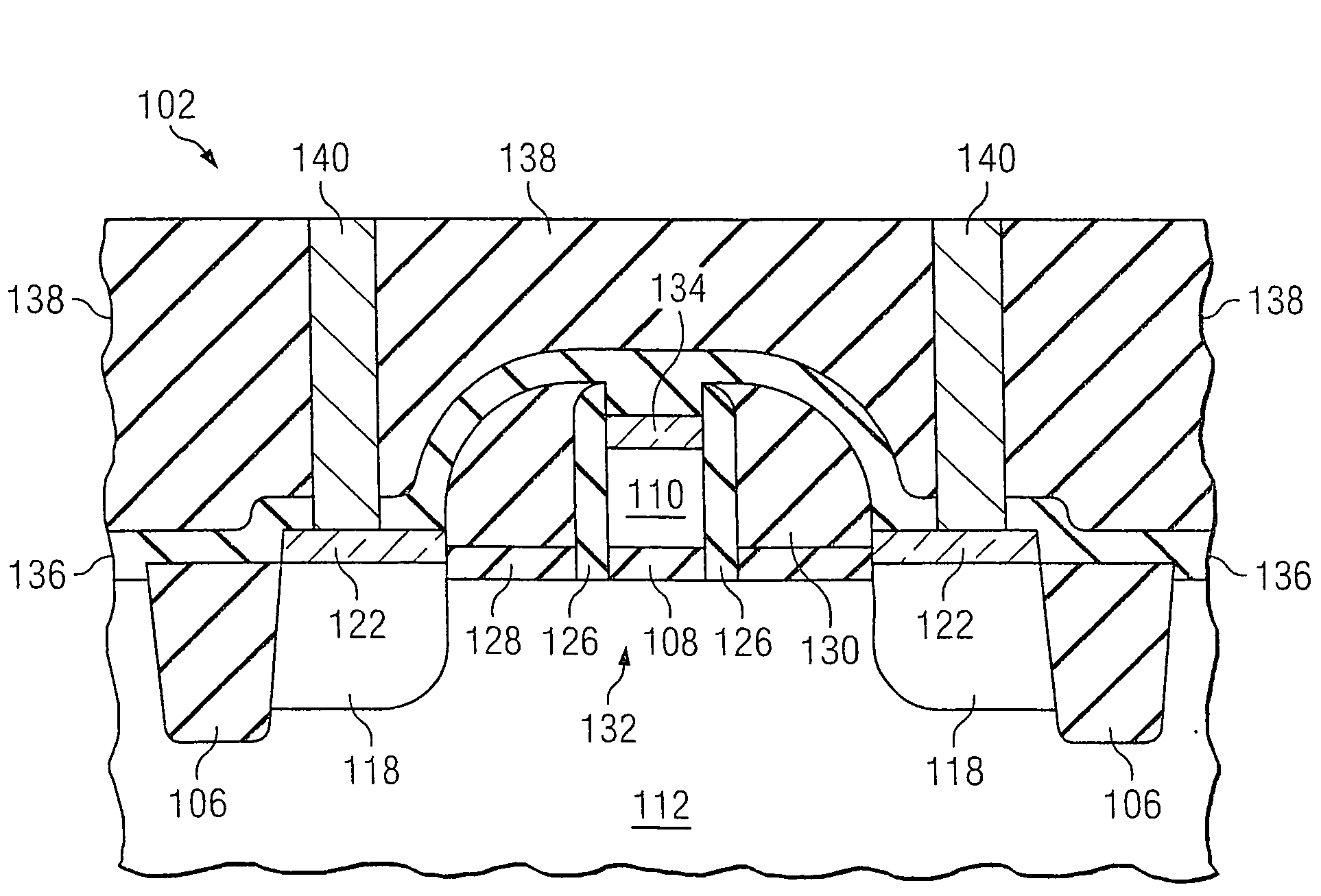
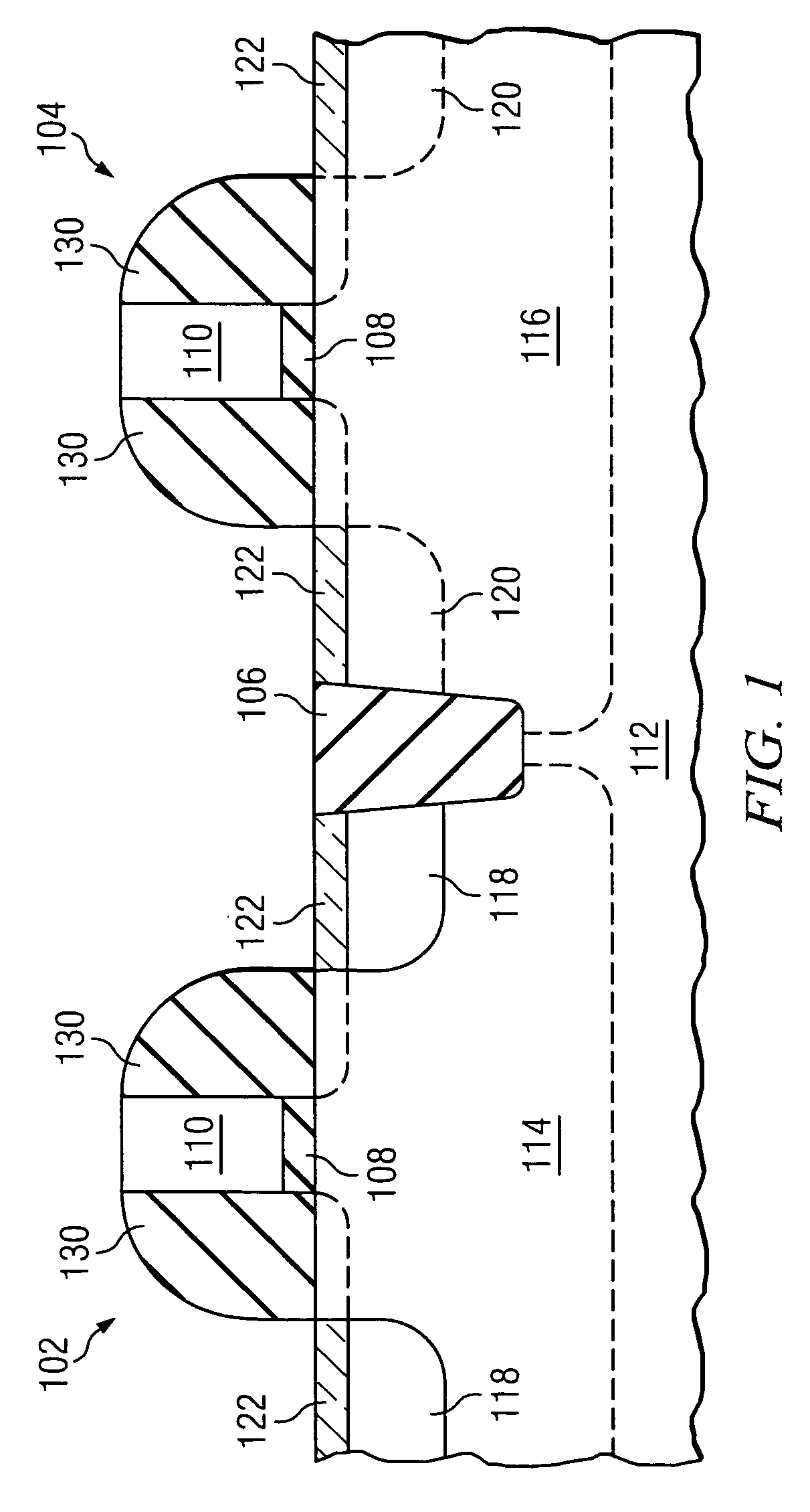
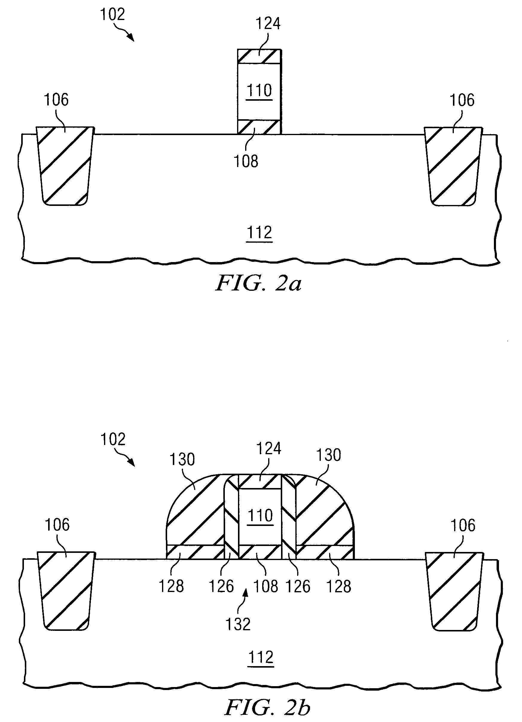
[0016]FIG. 1 illustrates a CMOS transistor pair that can utilize aspects of the present invention. The transistor pair includes a p-channel (PMOS) transistor 102 that is spaced from an n-channel transistor 104 by an isolation regio...


PUM


Abstract

In a method of making a semiconductor device, a recess is formed in an upper surface of the semiconductor body of a first material. An embedded semiconductor region is formed in the recess. The embedded semiconductor region is formed from a second semiconductor material that is different than the first semiconductor material. An upper surface of the embedded semiconductor region is amorphized to create an amorphous region. A silicide is then formed over the amorphous region.

Description

TECHNICAL FIELD[0001]This invention relates generally to semiconductor devices and methods, and more particularly to a strained semiconductor device and a method of making the same.BACKGROUND[0002]Semiconductor devices are used in a large number of electronic devices, such as computers, cell phones and others. One of the goals of the semiconductor industry is to continue shrinking the size and increasing the speed of individual devices. Smaller devices can operate at higher speeds since the physical distance between components is smaller. In addition, higher conductivity materials, such as copper, are replacing lower conductivity materials, such as aluminum. One other challenge is to increase the mobility of semiconductor carriers such as electrons and holes.[0003]One technique to improve transistor performance is to strain (i.e., distort) the semiconductor crystal lattice near the charge-carrier channel region. Transistors built on strained silicon, for example, have greater charge...

Claims


Application Information

Patent Timeline
IPC IPC(8): H01L21/336H01L21/20
CPCH01L21/823807H01L21/823814H01L29/165H01L29/665H01L29/7848H01L29/66636H01L29/7834H01L29/7843H01L29/66545
Inventor KWON, O SUNGKWON, OH JUNGHAN, JIN-PINGUTOMO, HENRY
Owner IBM CORP
Why Eureka
Try Eureka