Capacitance difference detecting circuit

a detection circuit and capacitance technology, applied in capacitance measurement, resistance/reactance/impedence, instruments, etc., can solve the problems of long wiring between the sensor and the inverter input terminal, high power consumption, complex structure,

Inactive Publication Date: 2008-05-29
KK TOSHIBA
View PDF6 Cites 27 Cited by
  • Summary
  • Abstract
  • Description
  • Claims
  • Application Information

AI Technical Summary

Benefits of technology

[0054]a control amplifier that controls said charging current by outputting a control voltage, which is the output of said summing amplifier amplified by integration so that the output of said summing amplifier is equal to a constant reference value, to said current source,

Problems solved by technology

The conventional capacitance difference detecting circuit described above has a problem that the structure is complicated, and the power consumption is high, because the PLL circuit is used.
Furthermore, for the conventional capacitance difference detecting circuit, the common terminal of the variable capacitors has to be connected to an inverting input terminal (a virtual ground point) that is extremely sensitive to the operation of a switched capacitor amplifier.
Typically, the wiring between the sensor and the inverting input terminal is long and therefore is largely affected by a disturbance.
Furthermore, a parasitic capacitance on the wiring may cause the amplifier to oscillate and make the amplifier unusable.
Therefore, variations in on-resistance of the switches or variations in switching time may cause a large offset.

Method used


Image

  • Capacitance difference detecting circuit
  • Capacitance difference detecting circuit
  • Capacitance difference detecting circuit

Examples


embodiment 1

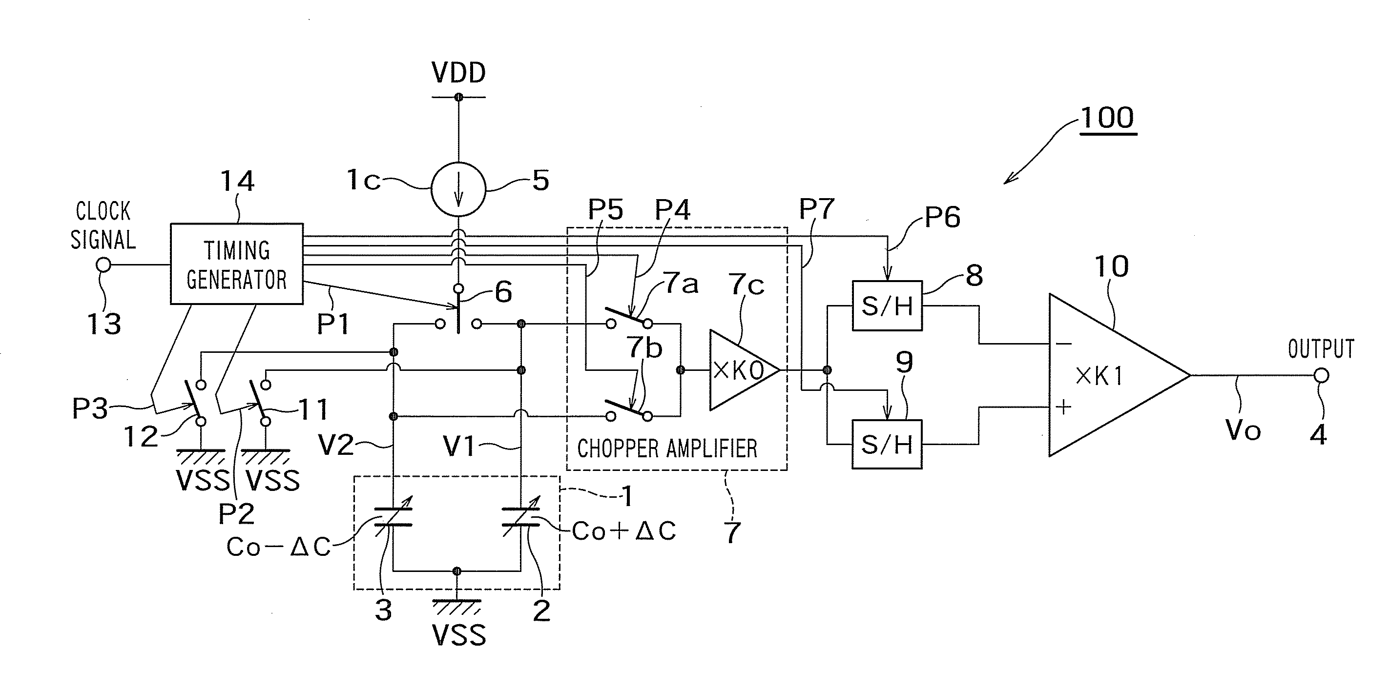
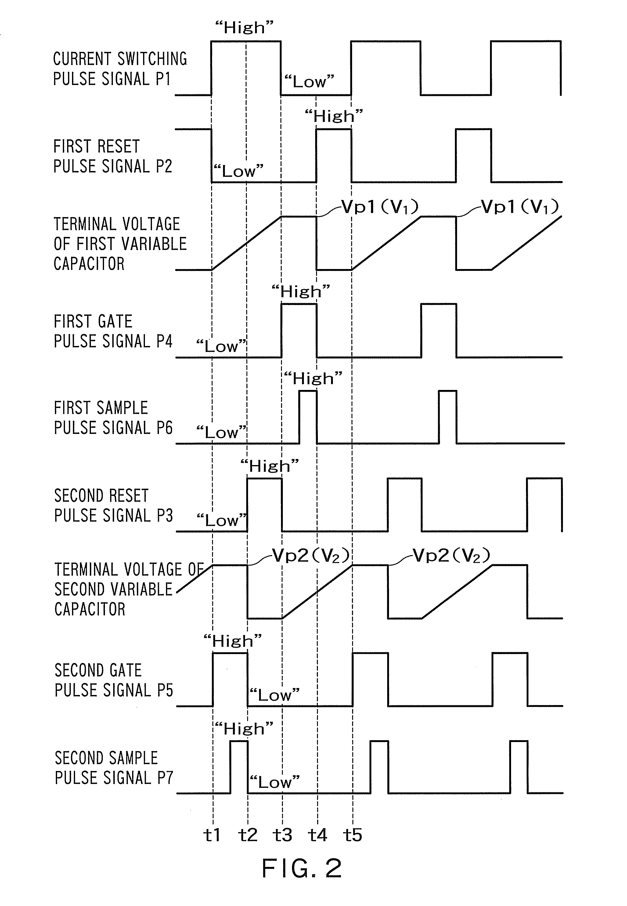
[0068]FIG. 1 is a diagram showing a configuration of essential parts of a capacitance difference detecting circuit according to an embodiment 1, which is an aspect of the present invention.

[0069]As shown in FIG. 1, a capacitance difference detecting circuit 100 detects the voltages for charging a first variable capacitor 2 and a second variable capacitor 3 forming a MEMS sensor 1, the sum of the capacitances of which is constant. The capacitance difference detecting circuit 100 outputs a signal corresponding to the detected voltages to an output terminal 4.

[0070]The capacitance difference detecting circuit 100 has a current source 5 that supplies a charging current to the first and second variable capacitors 2 and 3, and a current switching circuit 6 that is connected between the current source 5 and the first and second variable capacitors 2 and 3.

[0071]In this example, the current source 5 is a constant current source.

[0072]The current switching circuit 6 performs a switching oper...

embodiment 2

[0108]In the embodiment 1 described above, the current source that supplies a current to the variable capacitors is a constant current source.

[0109]In an embodiment 2, there will be described a configuration in which the current from the current source is adjusted so that the output of the capacitance difference detecting circuit is equal to a constant reference value.

[0110]FIG. 3 is a diagram showing a configuration of essential parts of a capacitance difference detecting circuit according to the embodiment 2, which is an aspect of the present invention. In this drawing, the same reference numerals as those in the embodiment 1 shown in FIG. 1 denote the same components as those in the embodiment 1.

[0111]As shown in FIG. 3, compared with the embodiment 1, a capacitance difference detecting circuit 200 further has a control amplifier 15 that sums the output of a first sampling and holding circuit 8 and the output of a second sampling and holding circuit 9, amplifies the sum value by ...

embodiment 3

[0120]In the embodiment 2, there has been described a configuration in which the current from the current source is adjusted so that the output of the capacitance difference detecting circuit is equal to a constant reference value.

[0121]In an embodiment 3, there will be described another configuration in which the current from the current source is adjusted so that the output of the capacitance difference detecting circuit is equal to a constant reference value.

[0122]FIG. 4 is a diagram showing a configuration of essential parts of a capacitance difference detecting circuit according to the embodiment 3, which is an aspect of the present invention. In FIG. 4, the components of a capacitance difference detecting circuit 300 other than those corresponding to the first and second sampling and holding circuits, the operational amplifier circuit and the control amplifier in the embodiment 2 shown in FIG. 3, which are different from those in the embodiment 2 shown in FIG. 3, are omitted b...


PUM


Abstract

A capacitance difference detecting circuit has timing generator that outputs a current switching pulse signal for controlling a switching operation of a current switching circuit, outputs a gate pulse signal for controlling a chopper amplifier so that the chopper amplifier detects the first charging voltage when a first variable capacitor is charged by a first charging voltage and detects a second charging voltage when a second variable capacitor is charged by a second charging voltage, outputs a first sample pulse signal for controlling a first sampling and holding circuit so that the first sampling and holding circuit samples and holds the output signal of the chopper amplifier when the first charging voltage is detected, and outputs a second sample pulse signal for controlling the second sampling and holding circuit so that the second sampling and holding circuit samples and holds the output signal of the chopper amplifier when the second charging voltage is detected.

Description

CROSS-REFERENCE TO RELATED APPLICATIONS[0001]This application is based upon and claims the benefit of priority from the prior Japanese Patent Application No. 2006-320159, filed on Nov. 28, 2006, and No. 2007-269968, filed on Oct. 17, 2007, the entire contents of which are incorporated herein by reference.BACKGROUND OF THE INVENTION[0002]1. Field of the Invention[0003]The present invention relates to a capacitance difference detecting circuit that detects a small change in capacitance of a micro electro mechanical systems (MEMS) sensor.[0004]2. Background Art[0005]A conventional capacitance difference detecting circuit that detects a small change in capacitance of a MEMS sensor has two LC resonance circuits using a sensor capacitance, a mixer circuit using the difference frequency therebetween, and an F / V converting circuit (a PLL circuit, for example) that converts the frequency of the output of the mixer circuit into voltage (see Japanese Patent Laid-Open No. 2005-326285, for examp...

Claims


Application Information

Patent Timeline
Patent Type & Authority Applications(United States)
IPC IPC(8): G01R27/26
CPCG01R27/2605
Inventor TAGUCHI, TOYOKI
Owner KK TOSHIBA
Why Eureka
Try Eureka