

Testing microelectronic devices using electro-optic modulator probes
a technology of electro-optic modulator and micro-electronic devices, applied in the direction of measuring devices, instruments, using optical means, etc., can solve the problems of power consumption or cooling resources, disturbance of signal integrity, and significant challenges encountered,
- Summary
- Abstract
- Description
- Claims
- Application Information
AI Technical Summary
Benefits of technology
Problems solved by technology
Method used
Image

Examples
Embodiment Construction
[0018]In the following description, numerous specific details are set forth. However, it is understood that embodiments of the invention may be practiced without these specific details. In other instances, well-known circuits, structures and techniques have not been shown in detail in order not to obscure the understanding of this description.
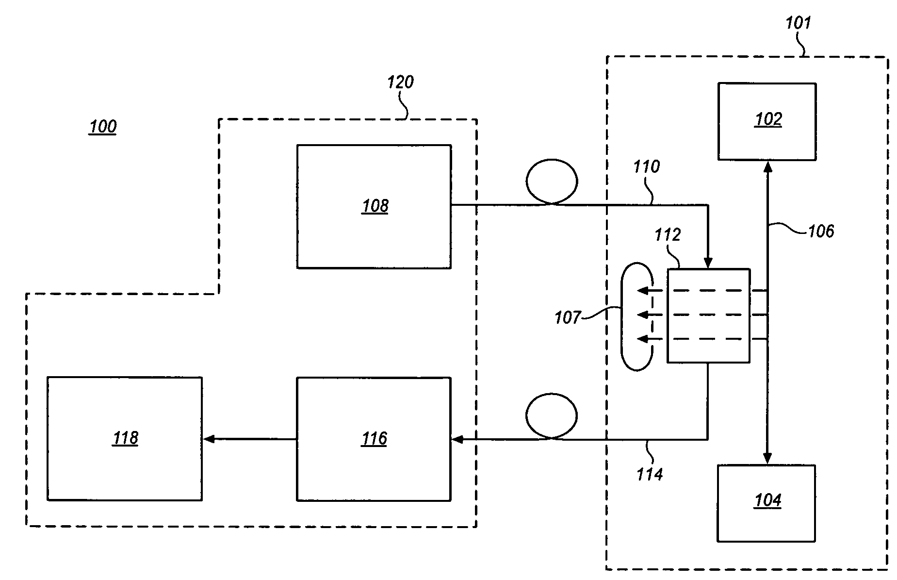
[0019]FIG. 1 is a block diagram of a test system 100 to test at least one microelectronic device 102, according to one or more embodiments of the invention. The test may be performed to debug, verify, optimize, validate, or otherwise test the microelectronic device.
[0020]The test system includes the at least one microelectronic device 102 to be debugged or otherwise tested. In one or more embodiments of the invention, the microelectronic device may include one or more microprocessors, graphics processors or other co-processors, controller chips or other chipset components, or other types of integrated circuits.
[0021]The microelectronic device i...
PUM
 Abstract
Description
Claims
Application Information