Array substrate for liquid crystal display device and method of manufacturing the same

a liquid crystal display and substrate technology, applied in semiconductor devices, optics, instruments, etc., can solve the problems of narrow viewing angle of lcd devices, decrease the probability of problems, etc., to prevent wavy noise on displayed images, reduce manufacturing costs and time, and minimize leakage current

Active Publication Date: 2008-05-29
LG DISPLAY CO LTD
View PDF10 Cites 25 Cited by
  • Summary
  • Abstract
  • Description
  • Claims
  • Application Information

AI Technical Summary

Benefits of technology

[0032]An object of embodiments of the invention is to provide an array substrate for an in-plane switching mode liquid crystal display device and a method of manufacturing the same that minimize leakage currents and prevent wavy noise on displayed images.
[0033]Another object is to provide an array substrate for an in-plane switching mode liquid crystal display device and a method of manufacturing the same that decrease manufacturing costs and time.

Problems solved by technology

However, the LCD device may have a narrow viewing angle.
The probability that problems may occur also decreases.

Method used


Image

  • Array substrate for liquid crystal display device and method of manufacturing the same
  • Array substrate for liquid crystal display device and method of manufacturing the same
  • Array substrate for liquid crystal display device and method of manufacturing the same

Examples


first embodiment

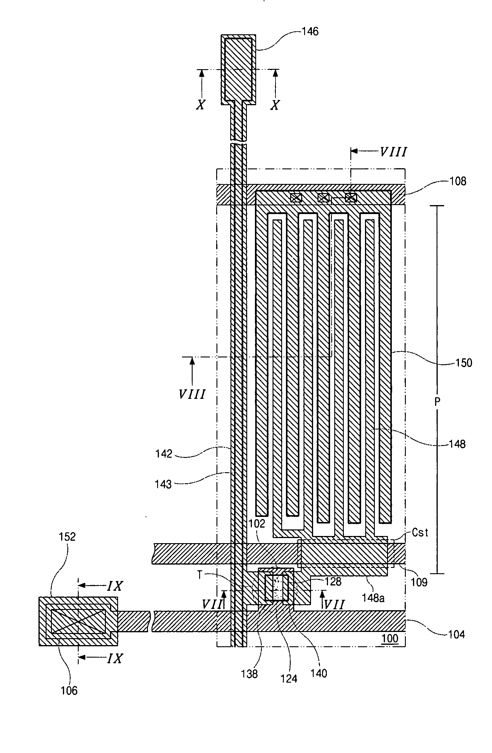
[0058]A method of manufacturing the array substrate will be explained hereinafter with reference to FIGS. 9A to 9I, FIGS. 10A to 10I, FIGS. 11A to 11I, and FIGS. 12A to 12I. FIGS. 9A to 9I are cross-sectional views along the line VII-VII of FIG. 7. FIGS. 10A to 10I are cross-sectional views along the line VIII-VIII of FIG. 7. FIGS. 11A to 11I are cross-sectional views along the line IX-IX of FIG. 7. FIGS. 12A to 12I are cross-sectional views along the line X-X of FIG. 7.

[0059]FIG. 9A, FIG. 10A, FIG. 11A and FIG. 12A show a first mask process. In FIG. 9A, FIG. 10A, FIG. 11A and FIG. 12A, a switching region S, a pixel region P, a gate region G, a data region D, and a common signal region CS are defined on a substrate 100. A first conductive metallic layer (not shown) is formed on the substrate 100, where the regions S, P, G, D and CS are defined, by depositing a conductive metal consisting of one or more material from a conductive metallic group including aluminum (Al), aluminum allo...

second embodiment

[0079]In the second embodiment, the pixel electrode 148′ and the common electrode 150′ are transparent, and thus the brightness of the device increases. In addition, since the drain electrode 140′ is transparent, light emitted from a backlight passes through the transparent drain electrode 140′. Accordingly, there is no light reflected by the drain electrode 140′ that goes into the active layer 124.

[0080]The array substrate according to the second embodiment may be manufactured through the same processes as the first embodiment except for the third conductive metallic layer is formed of a transparent conductive material, such as ITO or IZO.

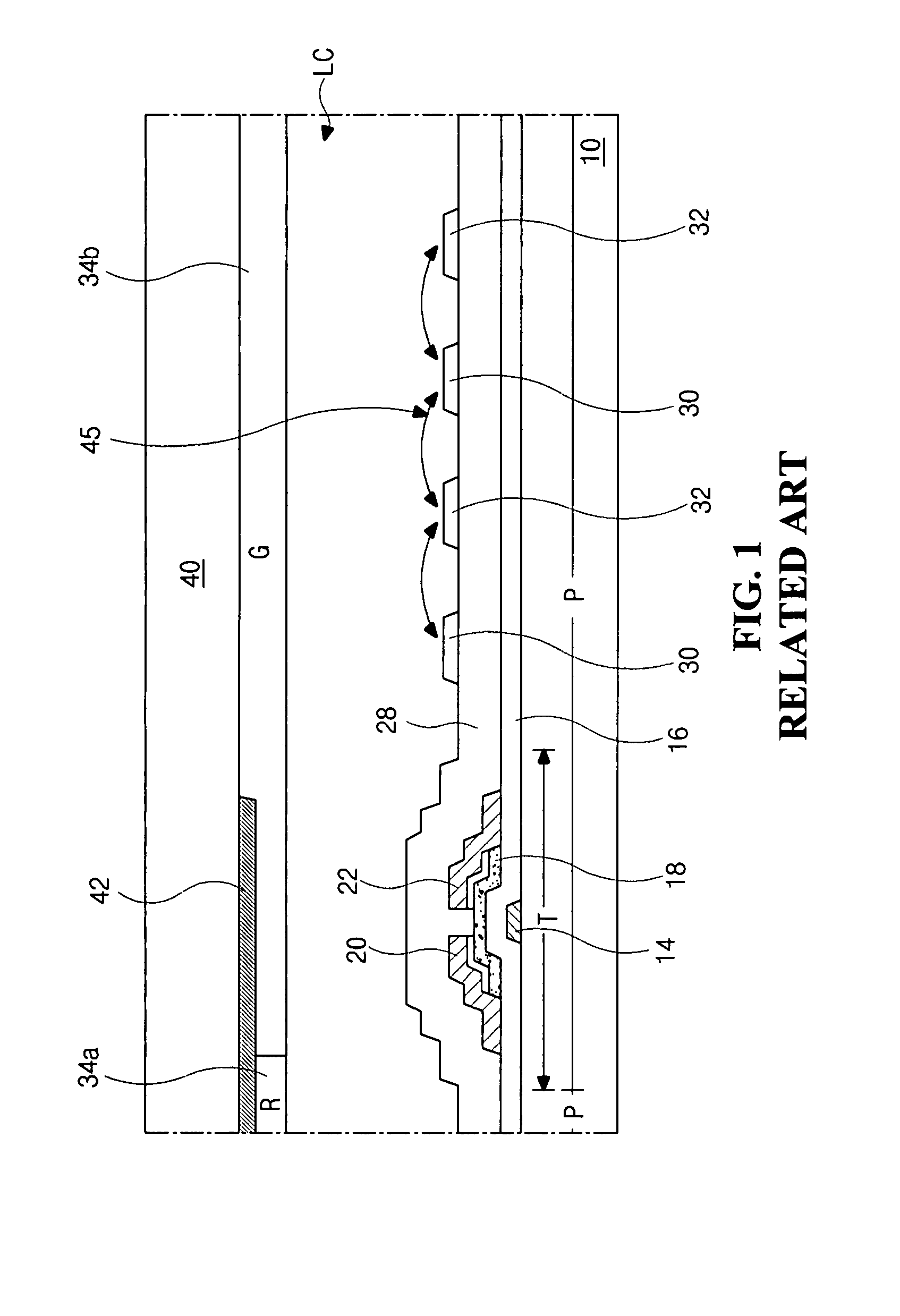
[0081]In the first and second embodiments, the passivation layer is formed by a liftoff method. In a third embodiment of the invention, the passivation layer is formed by using a shadow mask. A method of manufacturing an array substrate according to the third embodiment will be described hereinafter with reference to FIGS. 14A to 14C, FIGS. 15A to...


PUM


Abstract

An array substrate for a liquid crystal display device includes a substrate, a gate line on the substrate, a thin film transistor including a gate electrode of the gate line, a gate insulating layer over the gate electrode, an active layer on the gate insulating layer and ohmic contact layers on the active layer, and source and drain electrodes over the ohmic contact layers, a pixel electrode electrically connected to the drain electrode, a data line electrically connected to the source electrode and crossing the gate line, a common electrode spaced apart from the pixel electrode, and a passivation layer directly between the pixel electrode and the common electrode and directly between the source and drain electrodes.

Description

[0001]This application claims the benefit of Korean Patent Application Nos. 10-2006-0118593, filed in Korea on Nov. 28, 2006 and 10-2007-0039312, filed in Korea on Apr. 23, 2007, which are hereby incorporated by reference.BACKGROUND OF THE INVENTION[0002]1. Field of the Invention[0003]Embodiments of the present invention relate to a liquid crystal display device, and more particularly, to an array substrate for a liquid crystal display (LCD) device and a method of manufacturing the same.[0004]2. Discussion of the Related Art[0005]Liquid crystal display (LCD) devices are driven based on optical anisotropy and polarization characteristics of a liquid crystal material. Liquid crystal molecules have a long and thin shape, and the liquid crystal molecules are regularly arranged along in an alignment direction. Light passes through the LCD device along the long and thin shape of the liquid crystal molecules. The alignment of the liquid crystal molecules depends on the intensity or the dir...

Claims


Application Information

Patent Timeline
Patent Type & Authority Applications(United States)
IPC IPC(8): G09G3/30
CPCG02F1/134363H01L27/1288H01L27/1214G02F2001/136231G02F1/136231G02F1/133345G02F1/1339G09G3/36
Inventor LIM, JOO-SOOKIM, HYO-UKKWACK, HEE-YOUNGHONG, HYUN-SEOKAHN, BYUNG-CHULLIM, BYOUNG-HO
Owner LG DISPLAY CO LTD
Why Eureka
Try Eureka