Capacitor device

a capacitive couple and ceramic technology, applied in the field of ceramic capacitive couple improvement, can solve the problems of increasing the effort required to achieve these advances, reducing the capacitive density of multilayer ceramic capacitors or valve metal capacitors, and reducing the capacitive density. , to achieve the effect of reducing electrical shorts and leakage current, and increasing capacitan

Inactive Publication Date: 2008-05-29
KEMET ELECTRONICS CORP
View PDF14 Cites 19 Cited by
  • Summary
  • Abstract
  • Description
  • Claims
  • Application Information

AI Technical Summary

Benefits of technology

[0007]It is another object of the present invention to provide a capacitive couple with the interior areas of the anode covered by ceramic dielectric and a method for insuring complete coverage of the interior.
[0008]It is another object of the present invention to provide a capacitive couple comprising a porous anode from a conductor such as a valve metal with a sufficient covering of dielectric on the interior surface of the porous body to eliminate electrical shorts and leakage current.
[0009]A particular feature of the present invention is the increase in capacitance as a function of volume without loss of electrical properties.

Problems solved by technology

This effort is often contradictory to the companion desire to increase the capabilities of the electronic components.
For many of the components it is difficult to achieve further miniaturization without sacrificing electrical performance.
Furthering the capacitive density of either multilayer ceramic capacitors or valve metal capacitors is getting increasingly more difficult due to the extensive amount of effort already applied over many years by many researchers.
While there may still be advances forthcoming, the effort required to achieve these advances is becoming more difficult and further improvements may be approaching a plateau.
It is difficult to effectively introduce the dielectric, or polymeric cathode material, into the interior of the porous anode.
As a result the interior is not completely covered, which leads to shorts and high leakage current in capacitors of this nature.
Utilization of this technique has not been considered feasible on a large scale due to the high level of losses which occur with incomplete coverage of the interior of the porous anode body.

Method used


Image

  • Capacitor device
  • Capacitor device
  • Capacitor device

Examples


Embodiment Construction

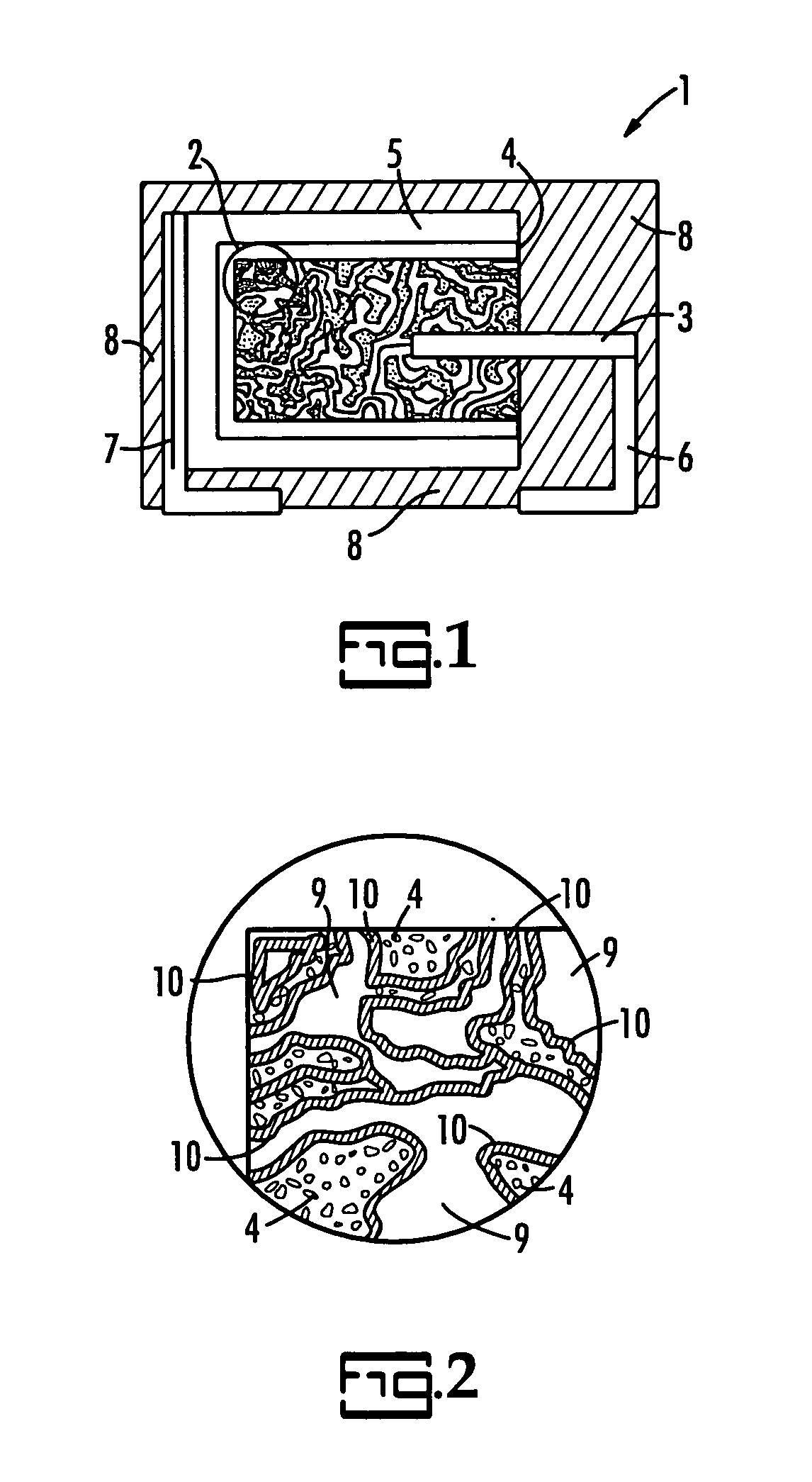
[0018]The invention will be described with reference to the figures forming an integral part of the instant application.

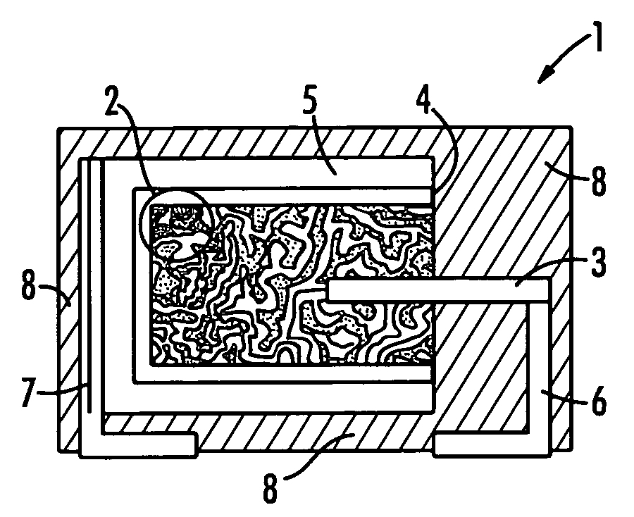
[0019]A capacitor of the present invention is illustrated in cross-sectional view in FIG. 1. In FIG. 1, the capacitor, generally represented at 1, comprises a porous anode, 2, with dielectric in the pores of the anode which are not visible in this view. An anode lead wire, 3, extends from the anode and is in electrical contact with the anode. The anode lead wire is typically pressed into the anode or welded to the anode. A cathode layer, 4, extends from the interior of the anode to the exterior as will be more readily understood from the description infra. The anode, dielectric and cathode form a capacitive couple which can be incorporated into a device such as a capacitor. An adhesive layer, 5, allows the cathode to be electrically connected to a cathode lead, 7. The adhesive layer may include multiple layers to allow adequate adhesion and conductivity from the ca...


PUM

PropertyMeasurementUnit
porosityaaaaaaaaaa
thicknessaaaaaaaaaa
thicknessaaaaaaaaaa

Abstract

A process for forming a capacitive couple. The process includes forming a highly porous body of a conducting material with interior struts and voids in electrical contact. A dielectric layer is formed in the voids on the struts with a material having a dielectric constant above 100. An insulating layer is formed on the struts not covered by the dielectric layer. A conductive layer is formed on the dielectric layer and on the insulating layer.

Description

BACKGROUND OF THE INVENTION[0001]The present invention is related to improvements in ceramic capacitive couples and devices comprising capacitive couples. More specifically, the present invention is related to a method for forming ceramic capacitive couples comprising dielectric in the interstitial spaces of a porous anode and a method for improving the capacitance achievable in a given volume by increasing the coverage of the interstitial spaces.[0002]The growth in electronic components has continued for many decades. One of the ongoing efforts is the continued push towards miniaturization of electronic circuitry and the components contained therein. This effort is often contradictory to the companion desire to increase the capabilities of the electronic components. For many of the components it is difficult to achieve further miniaturization without sacrificing electrical performance. This is particularly the case with capacitors or components comprising capacitive couples. There ...

Claims


Application Information

Patent Timeline
Patent Type & Authority Applications(United States)
IPC IPC(8): H01G9/00
CPCH01G9/0029H01G9/0032Y10T29/417H01G9/15H01G9/04
Inventor RANDALL, MICHAEL S.BLAIS, PETERPINCELOUP, PASCALSKAMSER, DANIEL J.GURAV, ABHIJITTAJUDDIN, AZIZUDDINKINARD, JOHN T.LESSNER, PHILIP
Owner KEMET ELECTRONICS CORP
Why Eureka
Try Eureka