Two-step self-aligned source etch wtih large process window

Active Publication Date: 2008-06-05
SEMICON MFG INT (SHANGHAI) CORP
View PDF2 Cites 0 Cited by
  • Summary
  • Abstract
  • Description
  • Claims
  • Application Information

AI Technical Summary

Benefits of technology

[0010]According to various embodiments, the present invention provides an improved technique for performing etching process and offers numerous advantages over conventional techniques. According to a specific embodiment, the present invention provides a two-step SAS etching process that utilizes protective layers on sidewalls

Problems solved by technology

An IC fabrication facility can cost hundreds of millions, or even billions, of dollars.
Making devices smaller is very challenging, as each process used in IC fabrication has a limit.
While processes such as self-

Method used


Image

  • Two-step self-aligned source etch wtih large process window
  • Two-step self-aligned source etch wtih large process window
  • Two-step self-aligned source etch wtih large process window

Examples


Example

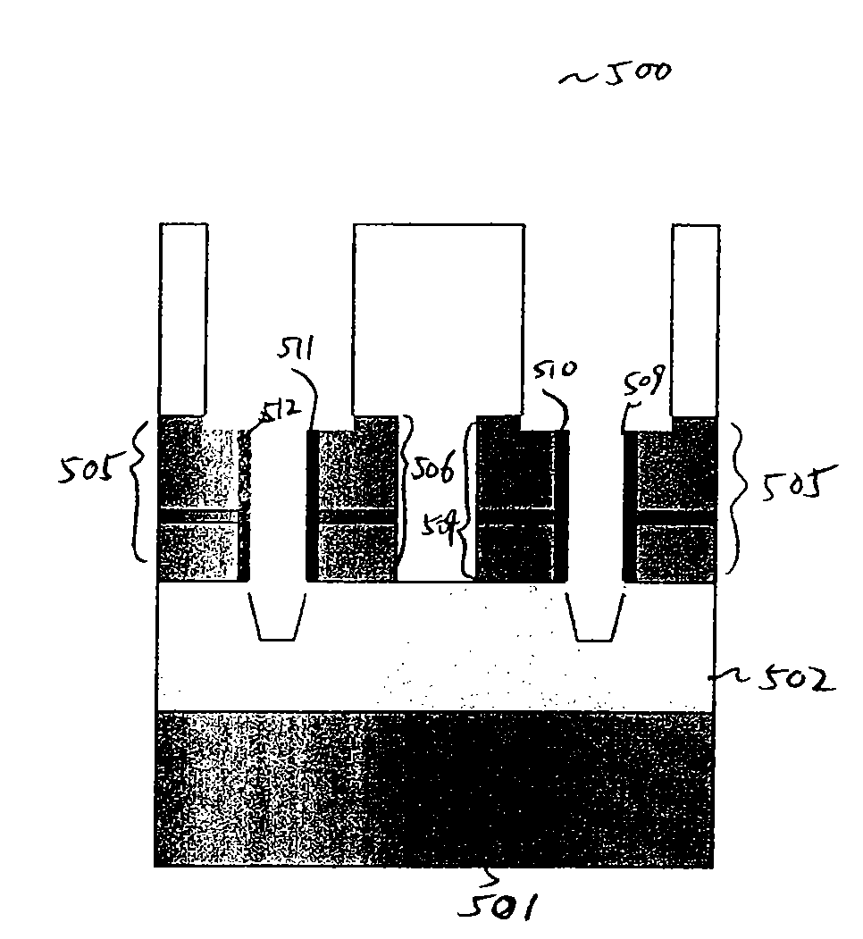
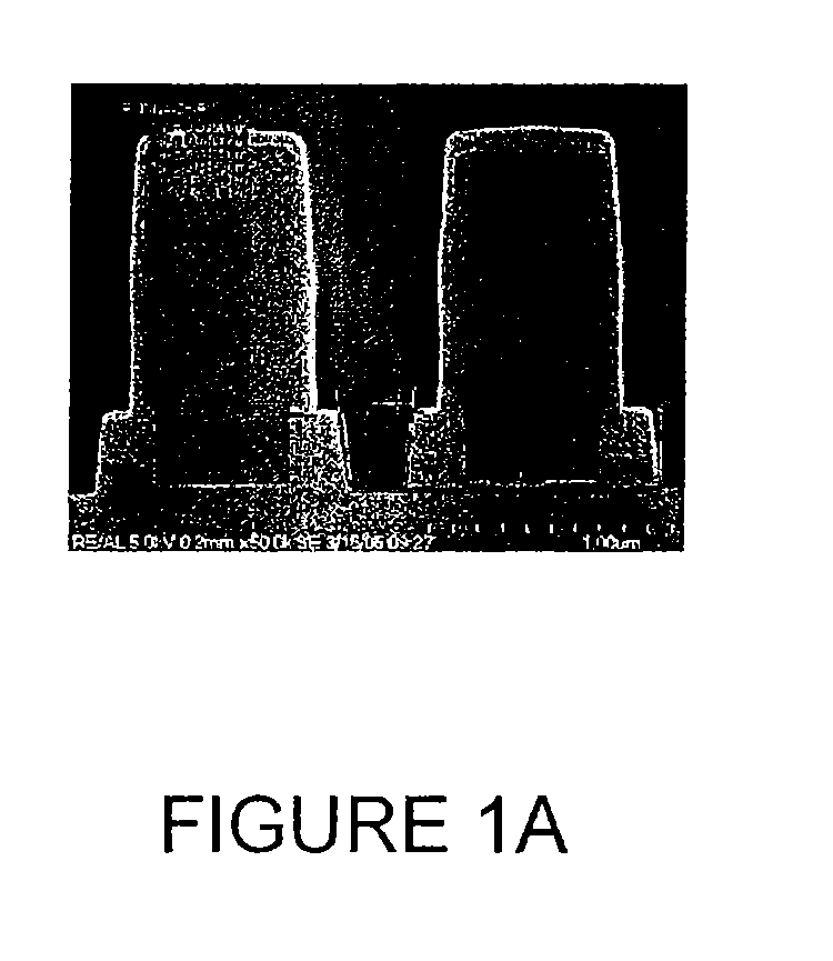
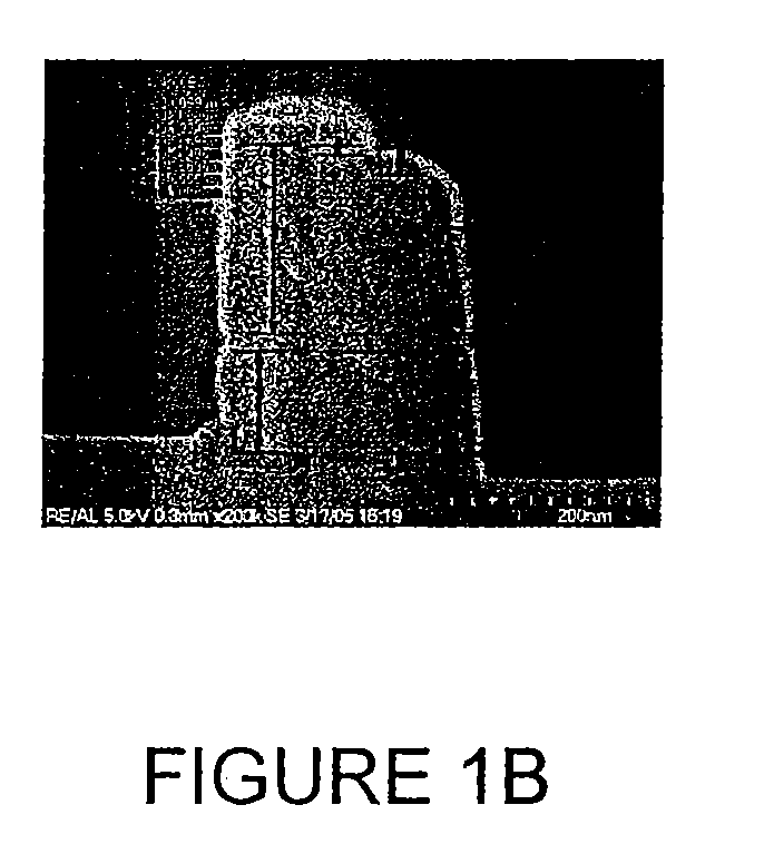
[0024]The present invention is directed to integrated circuits and their processing for the manufacture of semiconductor devices. In particular, the invention provides a method and device for self-aligned etching. Merely by way of example, the invention has been applied to the manufacturing of devices with decreased critical dimensions (e.g., devices characterized by channel lengths of less than 135 nanometers or even smaller). As an example, the invention can be used for the process of forming floating control gates on semiconductor devices. But it would be recognized that the invention has a much broader range of applicability. For example, an embodiment of the present invention can be used for the manufacturing of flash devices.

[0025]As discussed above, various techniques have been developed for the manufacturing of integrated circuits with small dimensions (e.g., 90 nanometers and 65 nanometers in channel lengths). For example, self-aligned source (SAS) etching process has been ...


PUM


Abstract

System and method for self-aligned etching. According to an embodiment, the present invention provides a method for performing self-aligned source etching process. The method includes a step for providing a substrate material. The method also includes a step for forming a layer of etchable oxide material overlying at least a portion of the substrate material. The layer of etchable oxide material can characterized by a first thickness. The layer of etchable oxide material includes a first portion, a second portion, and a third portion. The second portion is positioned between the first portion and the third portion. The method additionally includes a step for forming a plurality of structures overlying the layer of etchable oxide material. The plurality of structures includes a first structure and a second structure.

Description

CROSS-REFERENCES TO RELATED APPLICATIONS[0001]This application claims priority to Chinese Patent No. 200610119024.40 filed on Nov. 30, 2006 (SMIC Docket No. I-05-134), commonly assigned and hereby incorporated by reference for all purposes.BACKGROUND OF THE INVENTION[0002]The present invention is directed to integrated circuits and their processing for the manufacture of semiconductor devices. In particular, the invention provides a method and device for self-aligned etching. Merely by way of example, the invention has been applied to the manufacturing of devices with decreased critical dimensions (e.g., devices characterized by channel lengths of less than 135 nanometers or even smaller). As an example, the invention can be used for the process of forming floating control gates on semiconductor devices. But it would be recognized that the invention has a much broader range of applicability. For example, an embodiment of the present invention can be used for the manufacturing of fla...

Claims


Application Information

Patent Timeline
IPC IPC(8): H01L29/788H01L21/311H01L21/28
CPCH01L21/31116H01L21/31144H01L29/66636H01L29/0843H01L21/76897
Inventor HONG, ZHONGSHANLI, XUE
Owner SEMICON MFG INT (SHANGHAI) CORP
Why Eureka
Try Eureka