Edge exposure device

An edge exposure and edge technology, applied in the direction of photolithography exposure device, microlithography exposure equipment, etc., can solve the problem of no exposure size and dose monitoring, the problem of energy efficiency becomes particularly serious, and the method of adjusting the best focal plane is complicated And other issues

Active Publication Date: 2015-06-03
SHANGHAI MICRO ELECTRONICS EQUIP (GRP) CO LTD
View PDF6 Cites 6 Cited by
  • Summary
  • Abstract
  • Description
  • Claims
  • Application Information

AI Technical Summary

Problems solved by technology

Since the energy loss has a quadratic relationship with the blocked area at the aperture, the energy efficiency problem becomes particularly serious when the exposure field size is required to be adjustable.
The US Patent No. US2002 / 0092964A1 discloses another edge exposure system including an edge exposure lens and a distance sensor. The function of the distance sensor is to measure the distance from the lens to the surface of the silicon wafer, so as to adjust the position of the lens as a whole before exposure , this method of determining the focal plane is only the result of calibration conversion, and does not represent the real best focal plane, and the method of adjusting the best focal plane is slightly complicated, and there is no ability to monitor exposure size and dose

Method used


Image

  • Edge exposure device
  • Edge exposure device
  • Edge exposure device

Examples


Embodiment Construction

[0035] In order to make the above objects, features and advantages of the present invention more comprehensible, specific implementations of the present invention will be described in detail below in conjunction with the accompanying drawings. It should be noted that all the drawings of the present invention are in simplified form and use inaccurate scales, and are only used to facilitate and clearly assist the purpose of illustrating the embodiments of the present invention.

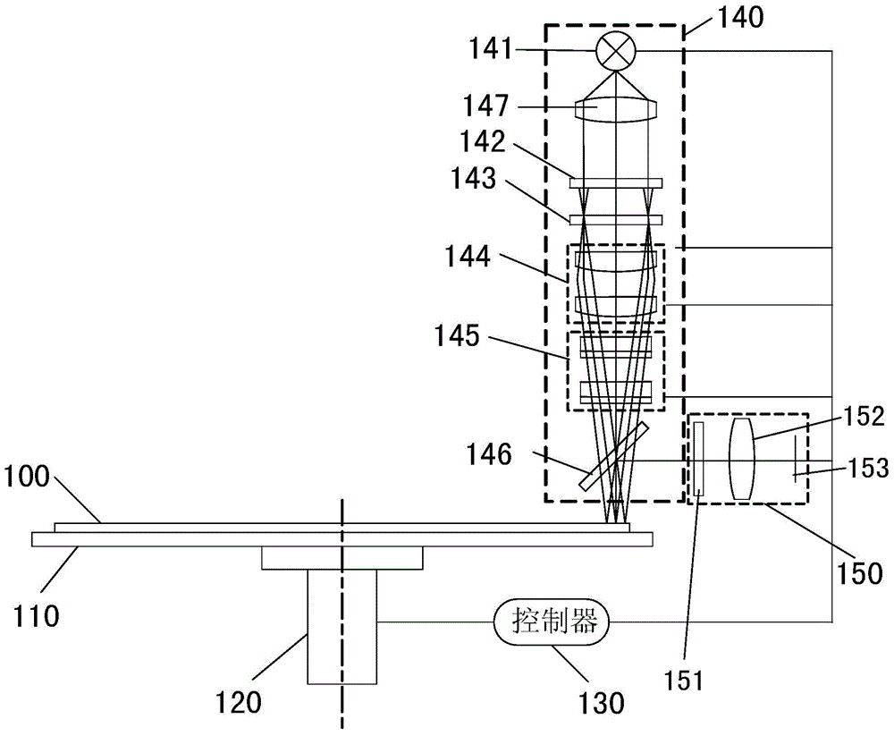
[0036] Please refer to Figure 3-6 , The edge exposure device of the present invention is mainly composed of four parts: the adsorption rotary table 110, the motor 120, the controller 130 and the edge exposure lens assembly. specifically,

[0037] The adsorption rotary table 110 is a device for absorbing and driving the silicon wafer 100 to rotate so as to perform edge exposure.

[0038] The motor 120 is a moving device that drives the rotation of the adsorption turntable 110 .

[0039] The controlle...


PUM


Abstract

The invention discloses an edge exposure device. The edge exposure device comprises an adsorption and rotating platform for adsorbing and driving a silicon chip to rotate, a motor for supplying power for the adsorption and rotating platform, an edge exposure lens assembly comprising an edge exposure camera lens and an exposure spot monitoring lens, wherein along an optical propagation direction, the edge exposure camera lens orderly comprises an exposure light source, first and second fly-eye lenses, a first cylindrical surface zoom lens group and a second cylindrical surface zoom lens group orthogonal to the first cylindrical surface zoom lens group, and a controller for controlling the motion of the motor, the edge exposure camera lens and the exposure spot monitoring lens. Through respective adjustment of combined focal length of the first cylindrical surface zoom lens group and the second cylindrical surface zoom lens group, edge exposure field length and width are controlled respectively, through cooperation of the first and second fly-eye lenses and the first and second cylindrical surface zoom lens groups, an exposure field is obtained, and through coaxial exposure field light spot imaging or energy detection light path, automatic focusing, exposure dosage and exposure size monitoring functions are obtained.

Description

technical field [0001] The invention relates to a silicon wafer edge exposure process, in particular to an edge exposure device. Background technique [0002] Wafer edge exposure (WEE) is one of the very important processes in the front-end manufacturing of IC circuits. Such as figure 1 and figure 2 As shown, due to the existence of cracks on the edge 11 of the silicon wafer, the gap 12 (Notch) in the judgment direction, the residue of photoresist, the pollutants from cleaning, the unevenness of coating, etching, and polishing, etc., the edge 11 of the silicon wafer cannot Use or even if the edge of the entire silicon wafer is covered with chips, it will still become a waste due to the problem of the edge 11 of the silicon wafer, which requires the photoresist on the edge 11 of the silicon wafer to be exposed and removed in advance. [0003] Electroplating In the subsequent packaging process of IC circuits, it is necessary to use the edge 11 of the silicon wafer as the a...

Claims


Application Information

Patent Timeline
Patent Type & Authority Applications(China)
IPC IPC(8): G03F7/20
Inventor 于大维潘炼东
Owner SHANGHAI MICRO ELECTRONICS EQUIP (GRP) CO LTD
Why Eureka
Try Eureka