Semiconductor structure with liner
a technology of semiconductors and structures, applied in semiconductor devices, semiconductor/solid-state device details, electrical apparatus, etc., can solve problems such as compounded problems, poor mechanical integrity of structures, and unsatisfactory thermal cycling and stress migration resistance of interconnect structures
- Summary
- Abstract
- Description
- Claims
- Application Information
AI Technical Summary
Problems solved by technology
Method used
Image

Examples
first embodiment
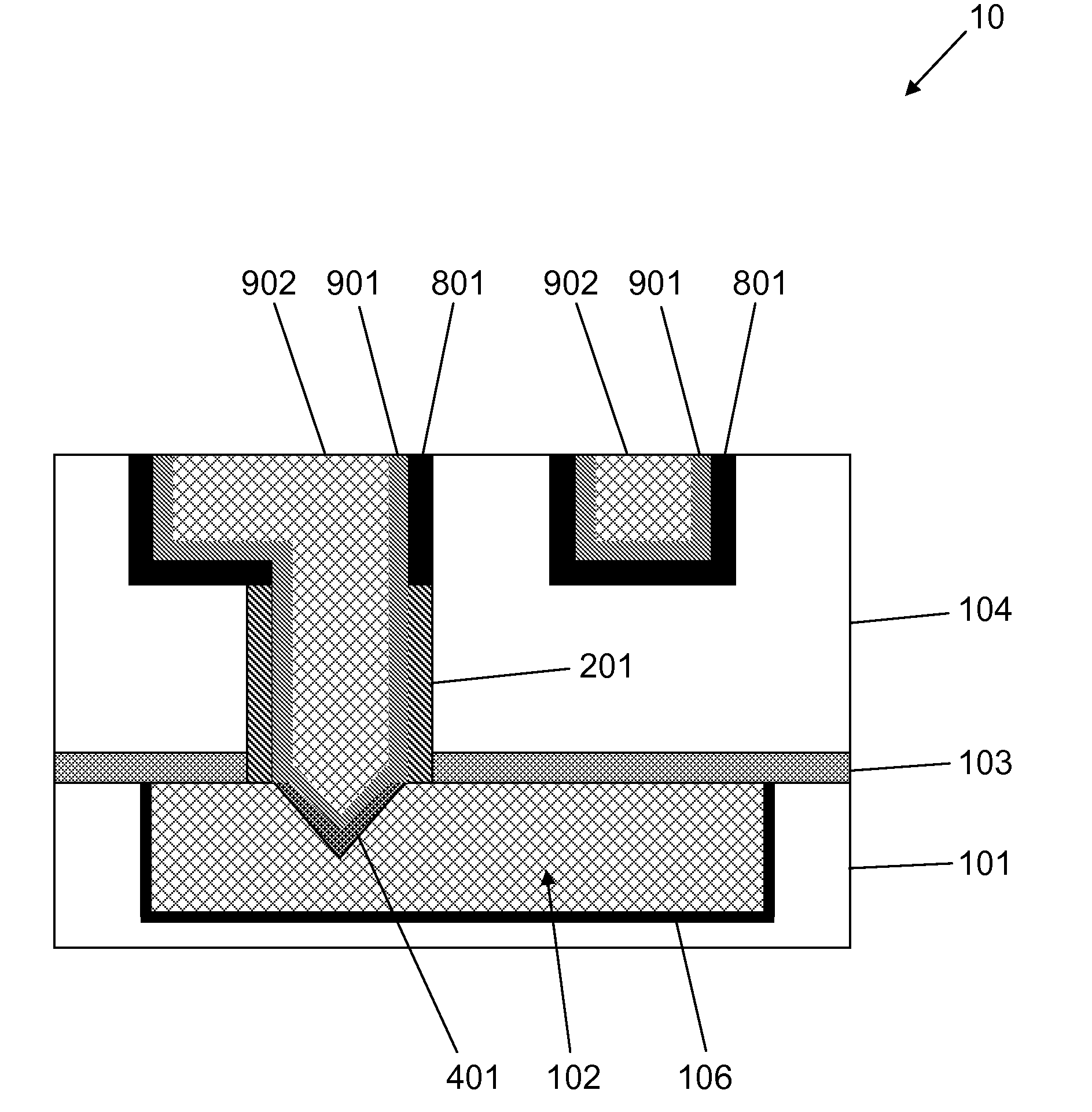
[0038]In embodiments, the liner 401 is left in place during filling of the contact via 107, gouging feature 300, and wire feature 600. For example, in a first embodiment shown in FIG. 8A, a diffusion barrier liner 801 is deposited over the exposed surfaces of the structure 10, except for the sidewalls of the contact via 107 and the liner 401 in the gouging feature 300. The diffusion barrier liner 801 may comprise, for example, Ta(N), Ti(N), W(N), Ru(N), or RuTa, and may have a thickness of about 2 nm to 60 nm, although other materials and thickness are contemplated for use with the invention. The material of the diffusion barrier liner 801 is applied by a non-directional deposition process that is capable of leaving the sidewalls of the contact via 107 and the liner 401 in the gouging feature 300 uncovered.
[0039]Still referring to the first embodiment, a copper seed layer 901 is deposited over the exposed surfaces of the contact via 107, gouging feature 300, and wire feature 600, as...
second embodiment
[0040]In a second embodiment shown in FIG. 9A, a diffusion barrier liner 801 is deposited over the exposed surfaces of the structure 10, including the sidewalls of the contact via 107 and the liner 401 in the gouging feature 300. The diffusion barrier liner 801 may comprise the same material and thickness range as described in references to FIG. 8A. The material of the diffusion barrier liner 801 is applied by a directional deposition process that covers the exposed surfaces of the structure 10.
[0041]Still referring to the second embodiment, a copper seed layer 901 is deposited over the exposed surfaces of the contact via 107, gouging feature 300, and wire feature 600, as shown in FIG. 9B. The copper seed layer 901 may be deposited in the same manner and thickness range as described with reference to FIG. 8B. Copper plating is used to fill the contact via 107, gouging feature 300, and wire feature 600 with copper material 902 in any suitable known fashion. Finally, the top surface o...
third embodiment
[0042]In other embodiments, the liner 401 is removed before subsequent filling of the contact via 107, gouging feature 300, and wire feature 600. For example, in a third embodiment shown in FIG. 10A, the liner 401 is removed by a sputtering process (such as that described with reference to FIG. 3) resulting in the exposure of the material of the interconnect feature 102 in the gouging feature 300. A diffusion barrier liner 801 is deposited over the exposed surfaces of the structure 10, except for the sidewalls of the contact via 107 and the exposed material in the gouging feature 300. The diffusion barrier liner 801 may comprise the same material and thickness range as described with reference to FIG. 8A. The material of the diffusion barrier liner 801 is applied by a non-directional deposition process that is capable of leaving the sidewalls of the contact via 107 and the exposed surfaces of the gouging feature 300 uncovered.
[0043]A copper seed layer 901 is deposited over the expos...
PUM
| Property | Measurement | Unit |
|---|---|---|
| dielectric constant | aaaaa | aaaaa |
| thickness | aaaaa | aaaaa |
| dielectric constant | aaaaa | aaaaa |
Abstract
Description
Claims
Application Information
 - Generate Ideas
- Intellectual Property
- Life Sciences
- Materials
- Tech Scout
- Unparalleled Data Quality
- Higher Quality Content
- 60% Fewer Hallucinations
Browse by: Latest US Patents, China's latest patents, Technical Efficacy Thesaurus, Application Domain, Technology Topic, Popular Technical Reports.
© 2025 PatSnap. All rights reserved.Legal|Privacy policy|Modern Slavery Act Transparency Statement|Sitemap|About US| Contact US: help@patsnap.com