

Touch panel
a technology of touch panel and display screen, which is applied in the field of touch panel, can solve the problems of affecting degrading the visibility of the display, and not providing sufficient suppression effect, and achieves good visibility, without display glare and color separation
- Summary
- Abstract
- Description
- Claims
- Application Information
AI Technical Summary
Benefits of technology
Problems solved by technology
Method used
Image

Examples
first embodiment
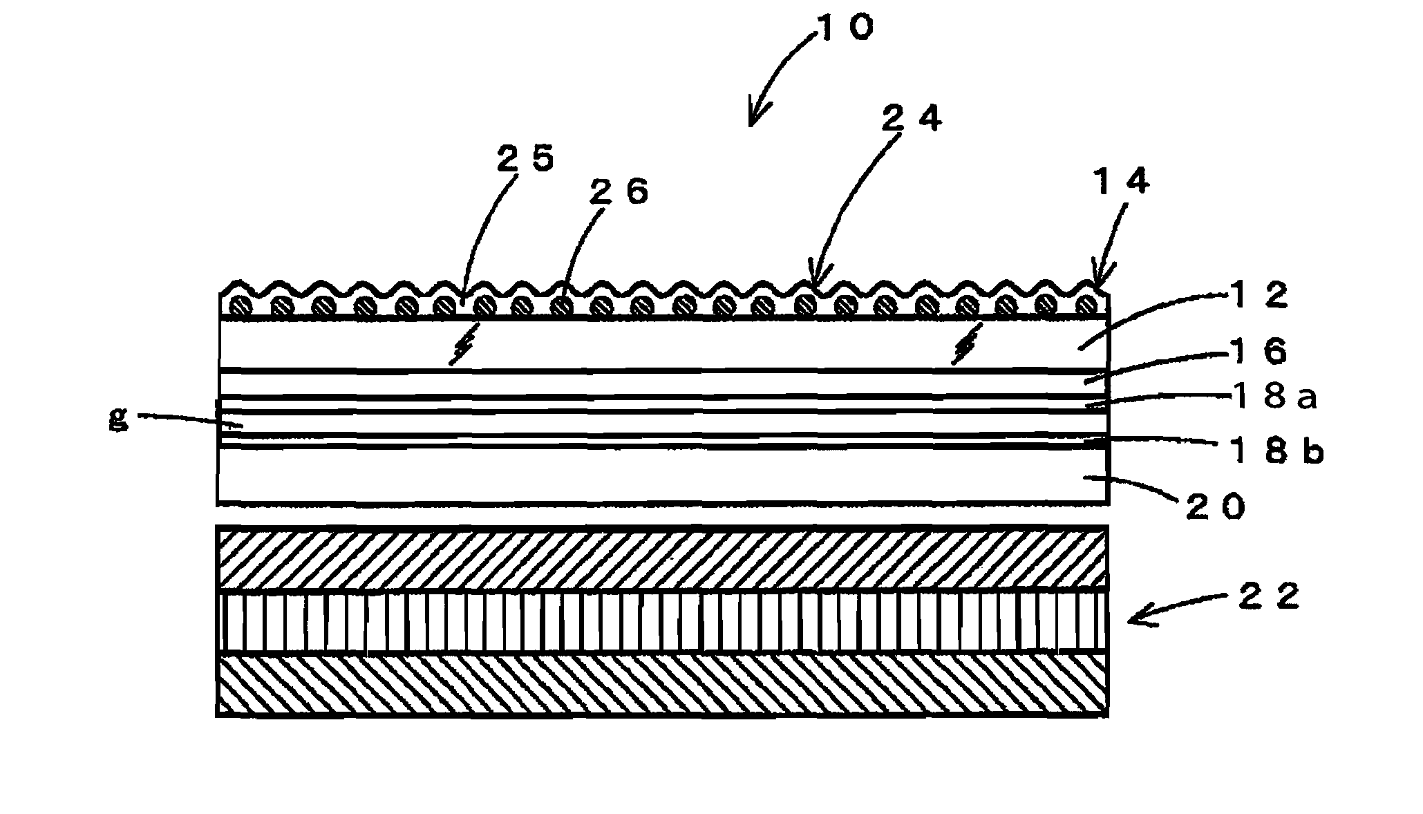
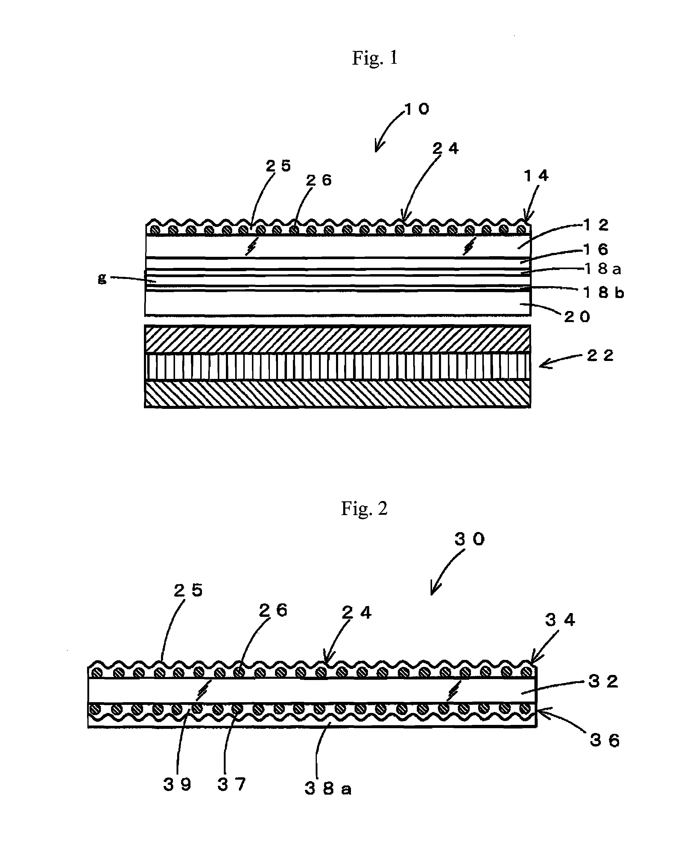
[0022]Embodiments of the present invention are described below with reference to the drawings. FIG. 1 shows the present invention wherein a touch panel 10 is provided with a touch panel film 14 comprising a film substrate 12 made of PET or the like and having a thickness of approximately 180 to 200 μm, for example. A transparent electrode 18a made of ITO film or the like is formed in a predetermined pattern on the rear surface of the touch panel film 14 with an anchor layer 16 disposed therebetween. The touch panel film 14 is affixed to the film substrate 12, which faces a touch panel substrate 20 on which a transparent electrode 18a and an opposing transparent electrode 18b are formed with a small gap therebetween. Then, the touch panel substrate 20 is affixed to the display surface of a liquid crystal or other display 22 formed from glass or transparent resin.
[0023]The film substrate 12 of the touch panel film 14 may be formed, for example, of polyethylene terephthalate (PET), or ...
second embodiment
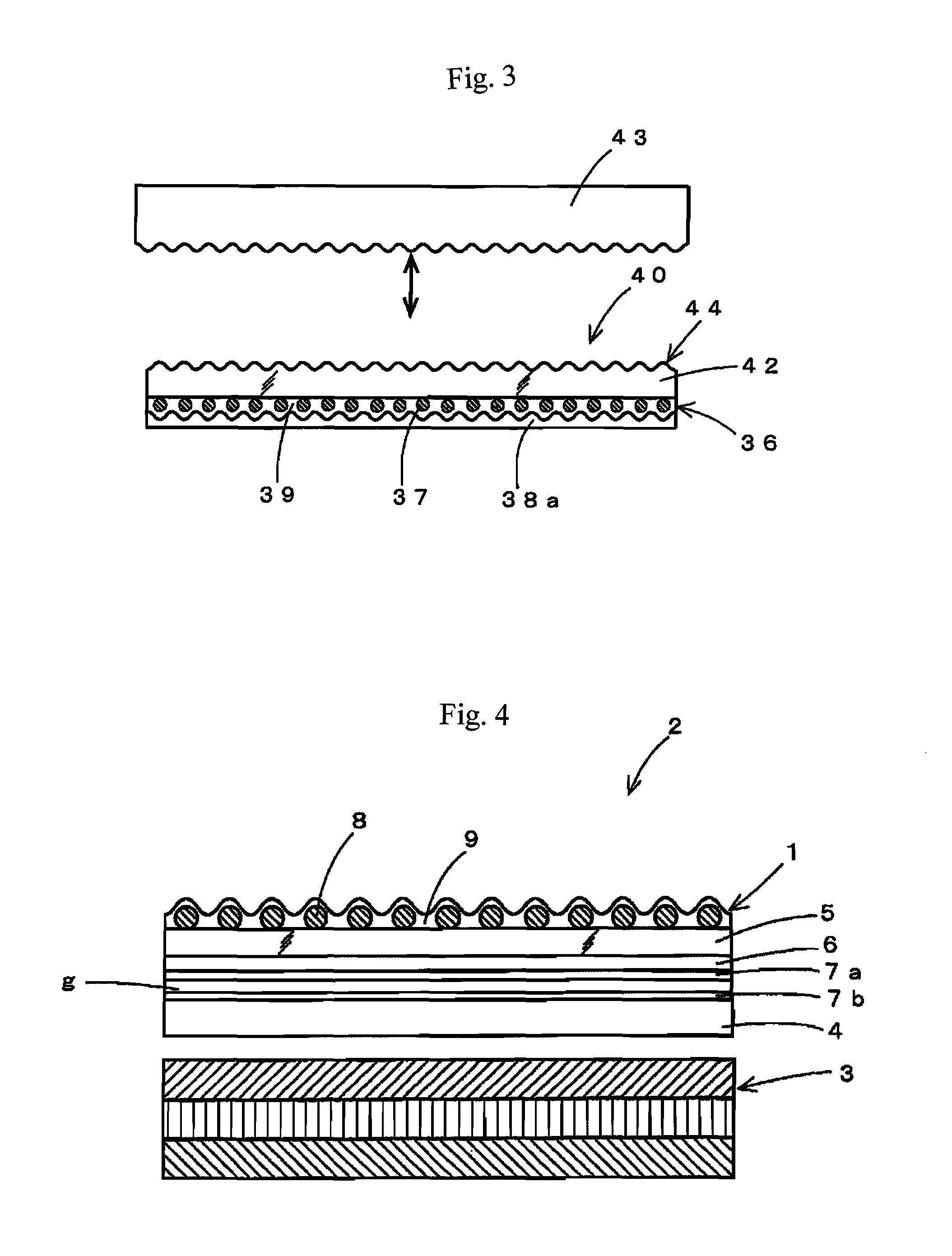
[0033]Similar to the second embodiment, an anchor layer 36 is also provided on the surface of the film substrate 42 on the touch panel side, and a transparent electrode 38a is formed in a predetermined pattern on the surface of the anchor layer 36. A filler 37, similar to that described above, of particles that are distributed and aligned substantially uniformly in a layer is provided within the curing resin 39 of the anchor layer 36, and the Ra of the anchor layer 36 is 0.1 μm to 0.01 μm. The arithmetic particle roughnesses (Ra's) on the front and rear surfaces of the touch panel film 44 are 1 / 2000th to 1 / 4000th of the pixel pitch of the display to which the touch panel is] attached.
[0034]The touch panel of the present invention is not limited to the above-described embodiments, and a number of methods for forming surface roughness may be selected as appropriate. In addition to the above-described use of a filler or of mold transfer, etching, sandblasting, embossing, and the like m...
PUM
 Abstract
Description
Claims
Application Information