Automatic testing method to be used by an IC testing system equipped with multiple testing sites

Inactive Publication Date: 2008-06-05
CHROMA ATE
View PDF1 Cites 0 Cited by
  • Summary
  • Abstract
  • Description
  • Claims
  • Application Information

AI Technical Summary

Benefits of technology

[0010]A primary objective of the present invention is to provide an automated testing method for an IC testing system with multiple testing sites with a reduced possibility of human error and need for human resources.
[0011]Another objective of the present invention is to provide an automated testing method for an IC testing system with multiple testing sites with high accuracy and efficiency. Another objective of the present invention is to provide an automated testing method for an IC testing system with multiple testing sites with reduced costs. Therefore, the automatic testing method to be used by an IC testing system equipped with multiple testing sites of the present invention, which could correspond to a plurality of testing circuit boards, wherein said testing circuit boards respectively correspond to a plurality of testing procedures whose numbers are less than those of the testing circuit boards, said testing system has a plurality of testing sites and a control device, said each testing site provides for installation of a testing circuit board respectively, and said testing circuit board has an ID code respectively; said method comprises installing the control device with a database of said each testing circuit board's ID code, testing procedure image files, and data linking each ID code to its pertinent image files; inputting the ID code of the testing circuit board of said each testing apparatus used in the test into said control device; providing the image file corresponding to said testing procedure, to which the testing circuit board of said each testing apparatus corresponds, for running said each testing apparatus by said control device. By using a central control module to control each testing apparatus and to send the correct testing process image file to each testing apparatus according to the testing circuit board's ID code, the role which human error may play in the testing process would be greatly reduced.

Problems solved by technology

Although the former method could thoroughly test the electrical properties of the IC, it also requires extensive hardware and software setup.
Not only does this setup require a lot of resources, it also requires a lot of time to reconfigure when an IC has its design updated.
Thus not only is this method costly, it is also hard to keep up with the rapidly changing electronic world.
Although this testing method takes a longer time, it easily determines the performance of the tested IC under actual usage and whether the IC is ready to be installed.
Yet there are some flaws in this testing method.
Hence this testing method requires a lot of manual effort and lacks efficiency.
Thus the hard drives are constantly turned on and off as the testing system tests one IC after another, which makes the hard drives very susceptible to failure due to cyclic loading.
If the wrong testing information is accidentally installed onto the hard drive, the testing procedure of the IC would be faulty.
At its least, this error may lead to the rejection of a perfectly capable IC.
At its worse, this error may lead to the acceptance of an incapable IC, which may lead to a faulty product line.
Whenever a change in the type of IC tested occurs, the information in the testing apparatuses must be updated, which makes the testing system vulnerable to the error described in the previous paragraph.
In addition, a single worker must often man more than one testing system, which increases the probability of the error occurring.

Method used


Image

  • Automatic testing method to be used by an IC testing system equipped with multiple testing sites
  • Automatic testing method to be used by an IC testing system equipped with multiple testing sites
  • Automatic testing method to be used by an IC testing system equipped with multiple testing sites

Examples


Embodiment Construction

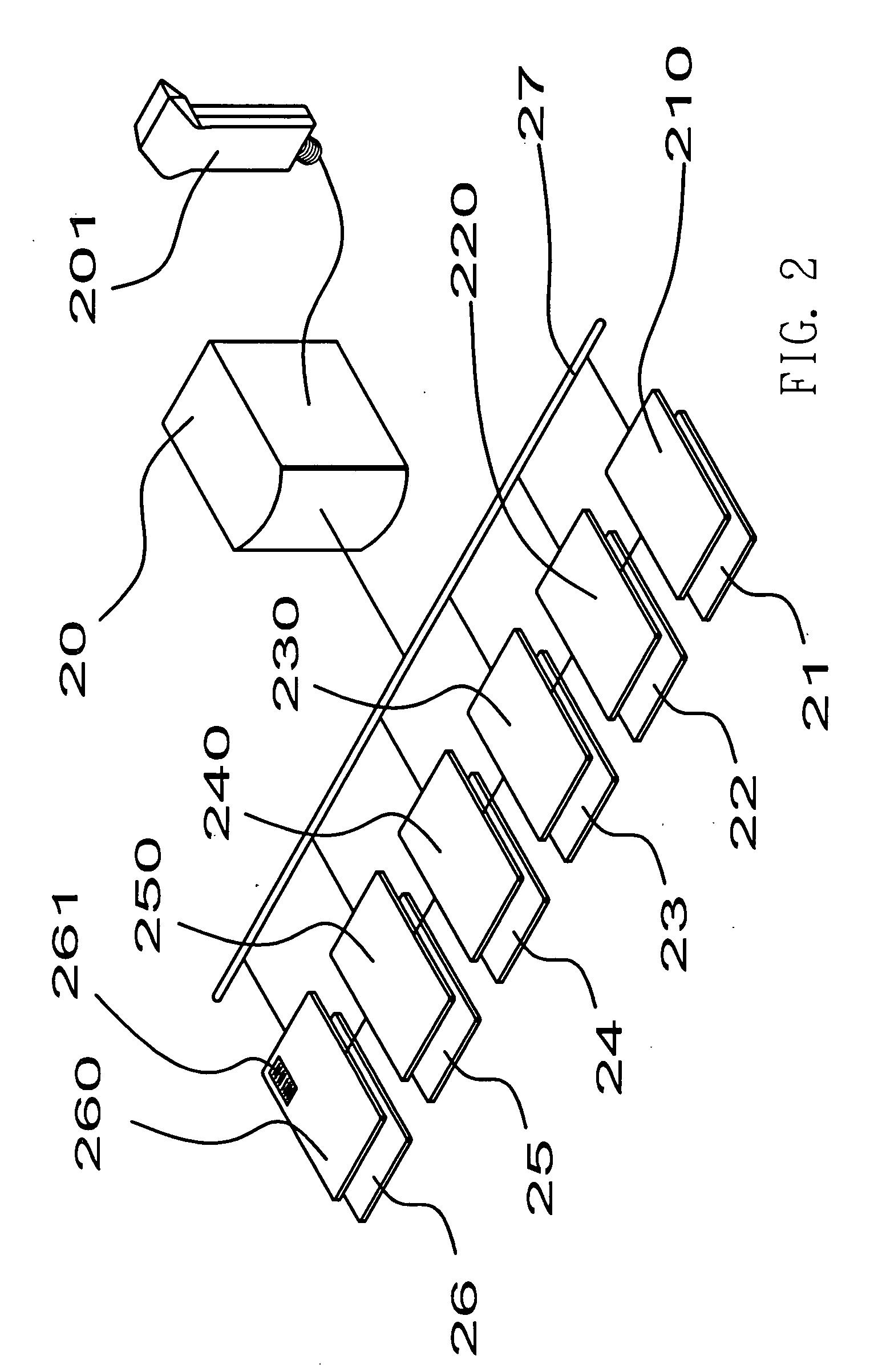
[0017]The first preferred embodiment of the automatic testing method to be used by an IC testing system equipped with multiple testing sites is shown in FIG. 2, which includes a control device 20, a bar code reading device 201, six testing apparatuses 21-26, and six separate testing circuit boards 210-260, one for each of the six testing apparatuses 21-26. Each testing circuit board 210-260 has an ID code. The control device 20 is connected via a communication means 27 to the testing circuit boards 210-260. The control device also has a device that could retrieve the ID codes from the circuit boards 210-260.

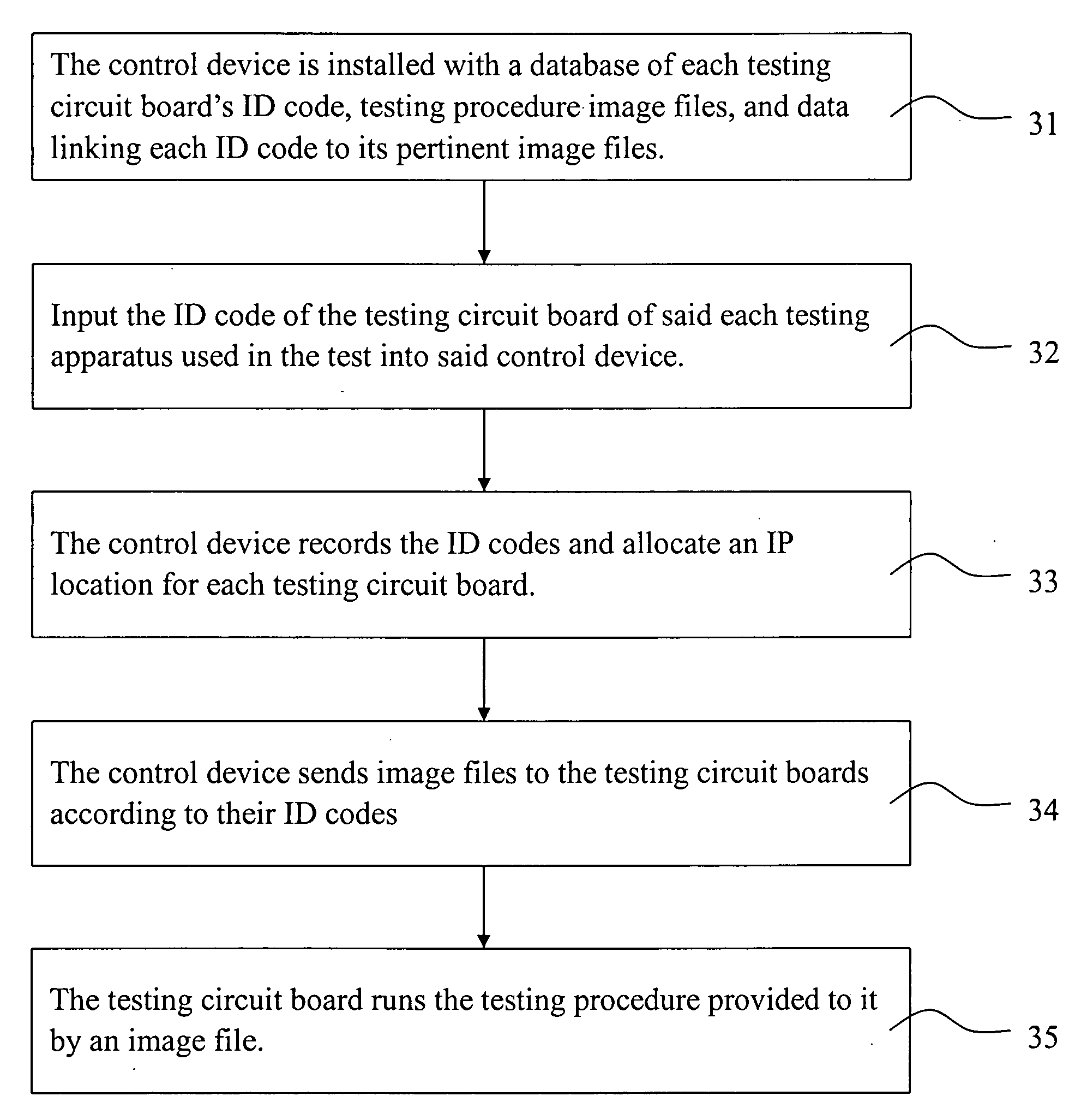
[0018]As shown in FIG. 3, before the testing system is run, the testing system must undergo step 31, where the control device 20 is installed with a database of each testing circuit board's ID code, testing procedure image files, and data linking each ID code to its pertinent image files. For example one testing system may need to test the CPU of a laptop, the IC of a video card,...


PUM


Abstract

An automatic testing method to be used by an IC testing system equipped with multiple testing sites. In this method the testing procedural information for each IC is stored in different sets of image files that are to be read by the testing system. Thus by inputting into the testing system the identification codes of the IC's that are going to be tested, the testing system would recognize which image files to use and the testing procedure would continue automatically. This method would greatly reduce the complex procedures needed to prepare an IC for testing in the prior art, thus leaving less room for human error and increasing the accuracy of the testing procedure.

Description

FIELD OF THE INVENTION[0001]This invention relates to an automatic testing method to be used by an IC testing system, more particularly to an automatic testing method to be used by an IC testing system which has its testing apparatuses boot, retrieve programs and run programs from a central control module, thus not requiring a hard disk, CD ROM drive or floppy disk drive to be installed for each apparatus.BACKGROUND OF THE INVENTION[0002]Integrated circuits have, without doubt, become the core of electronics nowadays. Consequently the reliability of an integrated circuit has a great impact on the reliability of the product it is utilized in.[0003]Currently IC testers could be categorized into 2 different types. One type of IC testers tests the electrical properties of the IC, while another type of IC testers tests the IC under actual usage. Although the former method could thoroughly test the electrical properties of the IC, it also requires extensive hardware and software setup. No...

Claims


Application Information

Patent Timeline
IPC IPC(8): G01R31/317G06K7/10
CPCG01R31/319
Inventor LAI, ANGUS
Owner CHROMA ATE
Why Eureka
Try Eureka