Nitride Semiconductor Light Emitting Device and Fabrication Method Thereof

Active Publication Date: 2008-06-12
SUZHOU LEKIN SEMICON CO LTD
View PDF3 Cites 21 Cited by
  • Summary
  • Abstract
  • Description
  • Claims
  • Application Information

AI Technical Summary

Benefits of technology

[0017]According to the present invention, the crystallinity of the active layer of the nitride semiconductor light emitting device can be enhanced, and the optical power and rel

Problems solved by technology

However, since Mg existing in the p—GaN layer has a low activation efficiency, it has a relatively high resistance value compared with the n—GaN layer used as the first electrode contact layer.
Due to the Mg atomic concentration remaining in the p—GaN layer without a complete activation, light emitting from the active layer toward the surface is trapped, or when a high current is applied, heat is generated due to a relatively high resistance value, so that the life time of the light emitting device is shortened to have a fatal influence on the reliability.
Especially, in the case of a large

Method used


Image

  • Nitride Semiconductor Light Emitting Device and Fabrication Method Thereof
  • Nitride Semiconductor Light Emitting Device and Fabrication Method Thereof
  • Nitride Semiconductor Light Emitting Device and Fabrication Method Thereof

Examples


Example

[0023]Hereinafter, an embodiment of the present invention will be described with reference to the accompanying drawings.

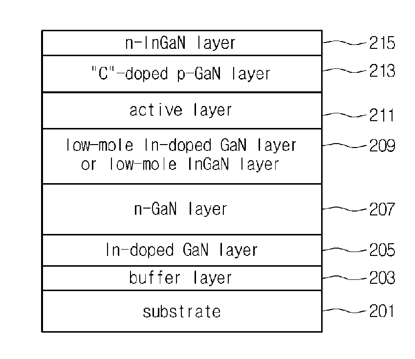
[0024]FIG. 1 is a sectional view of a nitride semiconductor light emitting device according to the present invention;

[0025]Referring to FIG. 1, the nitride semiconductor light emitting device according to the present invention includes a substrate 201, a buffer layer 203, an In-doped GaN layer 205, an n—GaN layer 207, a low-mole In-doped GaN layer or low-mole InGaN layer 209, an active layer 211, a “carbon (C)”-doped p—GaN layer 213, and an n—InGaN layer 215.

[0026]In the present invention, the buffer layer 203 is grown at a low growth temperature range of 500-600° C. on the substrate 201, for example, on a sapphire substrate. Herein, the buffer layer 203 can be formed in one selected from the group consisting of a stack structure of AlInN / GaN, a super lattice structure of InGaN / GaN, a stack structure of InxGal-xN / GaN, and a stack structure of AlxInYGal-(x+Y)N / InxGa...


PUM


Abstract

Provided is a nitride semiconductor light emitting device including: a first nitride semiconductor layer; an active layer formed above the first nitride semiconductor layer; and a “C (carbon)”-doped second nitride semiconductor layer formed above the active layer. According to the present invention, the crystallinity of the active layer is enhanced, and the optical power and the operation reliability are enhanced.

Description

TECHNICAL FIELD[0001]The present invention is relative to a nitride semiconductor light emitting device and fabrication method thereof, and to a nitride semiconductor light emitting device of which light output and operation reliability are enhanced, and a fabrication method thereof.BACKGROUND ART[0002]A schematic stack structure of a general nitride semiconductor light emitting device and a fabrication method thereof will now be described.[0003]A general nitride semiconductor light emitting device is provided in a stack structure including a substrate, a buffer layer, an n—GaN layer, an active layer and a p—GaN layer sequentially stacked from a lower side.[0004]In detail, in order to minimize the occurrence of crystal defects due to differences in the lattice constants and the thermal expansion coefficients of the substrate, for example, sapphire substrate, and the n—GaN layer, the buffer layer is formed of a GaN-based nitride or an AlN-based nitride having an amorphous phase at a ...

Claims


Application Information

Patent Timeline
IPC IPC(8): H01L33/00H01L33/06H01L33/12H01L33/32
CPCH01L33/025H01L33/325H01L33/14
Inventor LEE, SUK HUN
Owner SUZHOU LEKIN SEMICON CO LTD
Why Eureka
Try Eureka