

Nitride Semiconductor Light Emitting Device and Fabrication Method Therefor
- Summary
- Abstract
- Description
- Claims
- Application Information
AI Technical Summary
Benefits of technology
Problems solved by technology
Method used
Image

Examples
Embodiment Construction
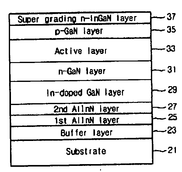
[0062]According to the spirit of the present invention, the performance of the single quantum well LED having the structure of ITO / n-InGaN layer / p-GaN layer / (InGaN / InGaN)SQW layer / n+-GaN(Si-In) layer / GaN(In) layer / (second AlInN layer / first AlInN layer) / (GaN / AlInN / GaN / AlInN)buffer layer / sapphire substrate was tested to obtain the following results. Herein, the n+-GaN(Si-In) layer is the first electrode contact layer, and the n-InGaN layer is the second electrode contact layer.
[0063]At the current of 20 mA, electrical performances, for example, the core wavelength of 460 nm, the light power of 6.3 mW, the operation voltage (VF) of 3.1 V were obtained. In the human body mode, the ESD value is at least −1 KV, of which 90% or more can be attained on the entire of a 2-inch sapphire substrate. Herein, the measurement values were measured using a blue LED chip die and especially the light power was measured using an integral sphere.
MODE FOR INVENTION
[0064]Although the nitride semiconductor...
PUM
 Abstract
Description
Claims
Application Information