

Film deposition method and manufacturing method of semiconductor device
- Summary
- Abstract
- Description
- Claims
- Application Information
AI Technical Summary
Benefits of technology
Problems solved by technology
Method used
Image

Examples
first embodiment
1. First Embodiment
First Example of Film Deposition Method
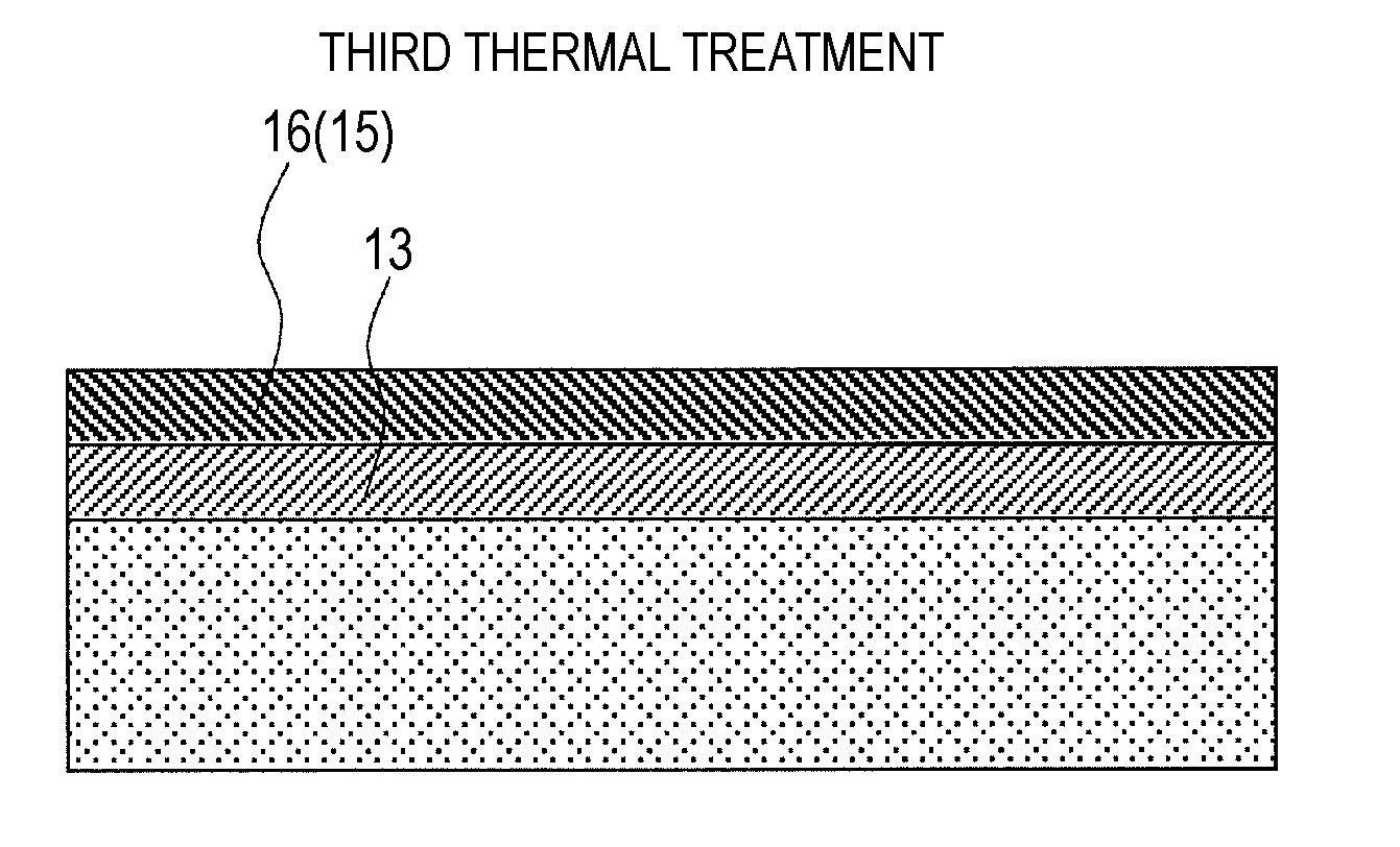
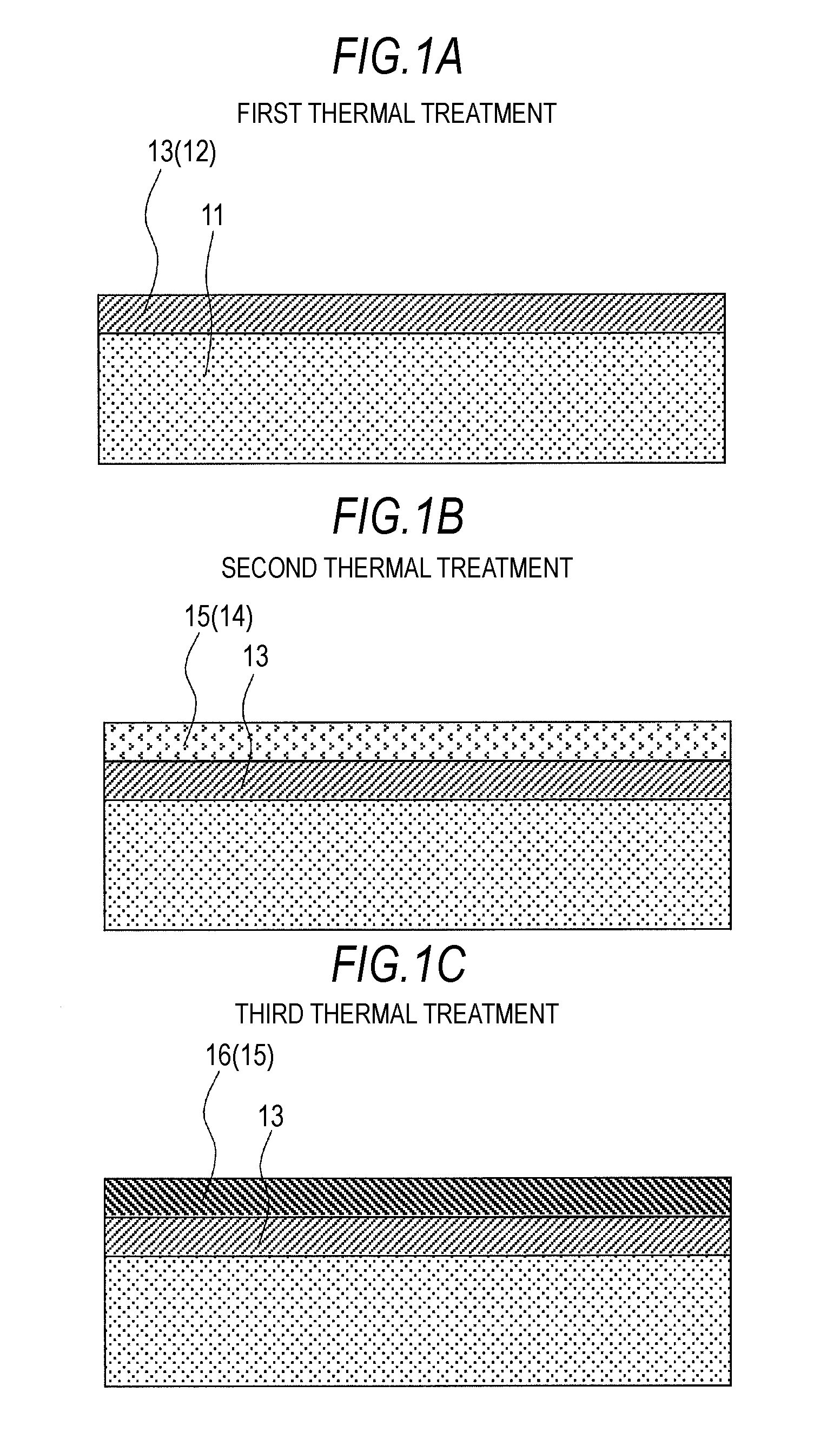
[0041]A first example of the film deposition method according to a first embodiment of the present invention is described with reference to a manufacturing step sectional view shown in each of FIGS. 1A to 1C.
[0042]As shown in FIG. 1A, a solution containing a polysilane compound is coated on a substrate 11 to form a coating film 12, which is then subjected to a first thermal treatment in an inert atmosphere, thereby forming the coating film 12 into a silicon film 13.
[0043]A step of forming the coating film 12 is preferably carried out in an inert atmosphere of argon, nitrogen or the like. Alternatively, hydrogen may be contained in a reducing atmosphere.
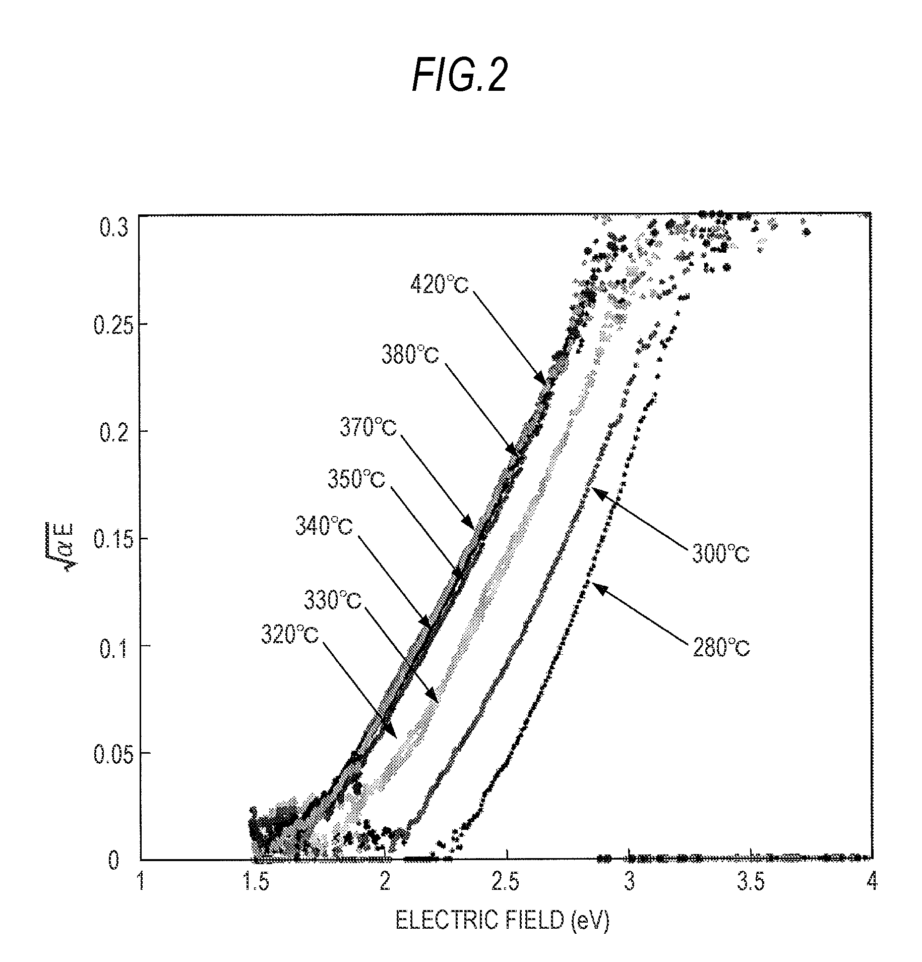
[0044]As shown in FIG. 2, when the first thermal treatment is carried out at a temperature of 300° C. or higher in an inert atmosphere of argon, nitrogen or the like, a band gap of the silicon film 13 becomes not more than 2 eV. The temperature at which it reaches a stable regi...
second embodiment
2. Second Embodiment
First Example of Manufacturing Method of Semiconductor Device
[0183]A first example of the manufacturing method of a semiconductor device according to the second embodiment of the present invention is described with reference to a schematic configuration sectional view shown in each of FIGS. 10A to 10F.
[0184]First of all, as shown in FIG. 10A, a solution containing a polysilane compound is coated on a substrate 11 to form a coating film 12, which is then subjected to a first thermal treatment in an inert atmosphere, thereby forming the coating film 12 into a silicon film 13 according to the film deposition method described above with reference to FIGS. 1A to 1C.
[0185]As the polysilane compound, those described above are useful.
[0186]That is, the polysilane compound is one represented by SinRm (wherein n represents a natural number of 3 or more; m is a number of (2n−2) or more and not more than (2n+2); and R represents an organic chain material, an organic cyclic m...
PUM
| Property | Measurement | Unit |
|---|---|---|
| Temperature | aaaaa | aaaaa |
| Temperature | aaaaa | aaaaa |
| Temperature | aaaaa | aaaaa |
Abstract
Description
Claims
Application Information