AlGaN substrate and production method thereof

Inactive Publication Date: 2006-10-12
SHOWA DENKO KK
View PDF5 Cites 11 Cited by
  • Summary
  • Abstract
  • Description
  • Claims
  • Application Information

AI Technical Summary

Benefits of technology

[0024] On the other hand, in the case of using AlGaN substrate having a composition permitting transmission of an emission wavelength, no light is absorbed in the substrate to heighten the luminous efficiency. In addition, since the difference in lattice constant and thermal expansion coefficient from the light-emitting layer becomes small, cracks are difficult to produce and the crystallinity is enhanced. When using the MOCVD method, it is possible to produce an AlGaN substrate excellent in composi

Problems solved by technology

In this method, however, it is difficult to suppress crack formation in a region having a large Al composition and, even when the crack formation can be suppressed, the dislocation density is large.
Thus, such a substrate cannot be used as the substrate for a light-emitting device.
However, since the growth speed in the MOCVD method is gener

Method used


Image

  • AlGaN substrate and production method thereof
  • AlGaN substrate and production method thereof
  • AlGaN substrate and production method thereof

Examples


Example

EXAMPLE 1

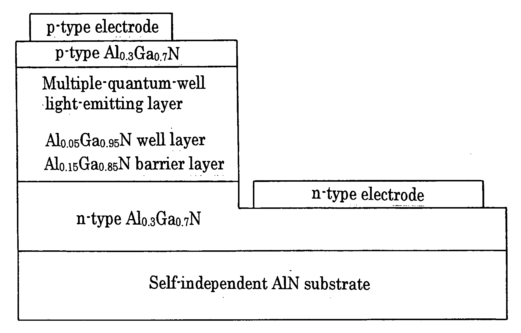
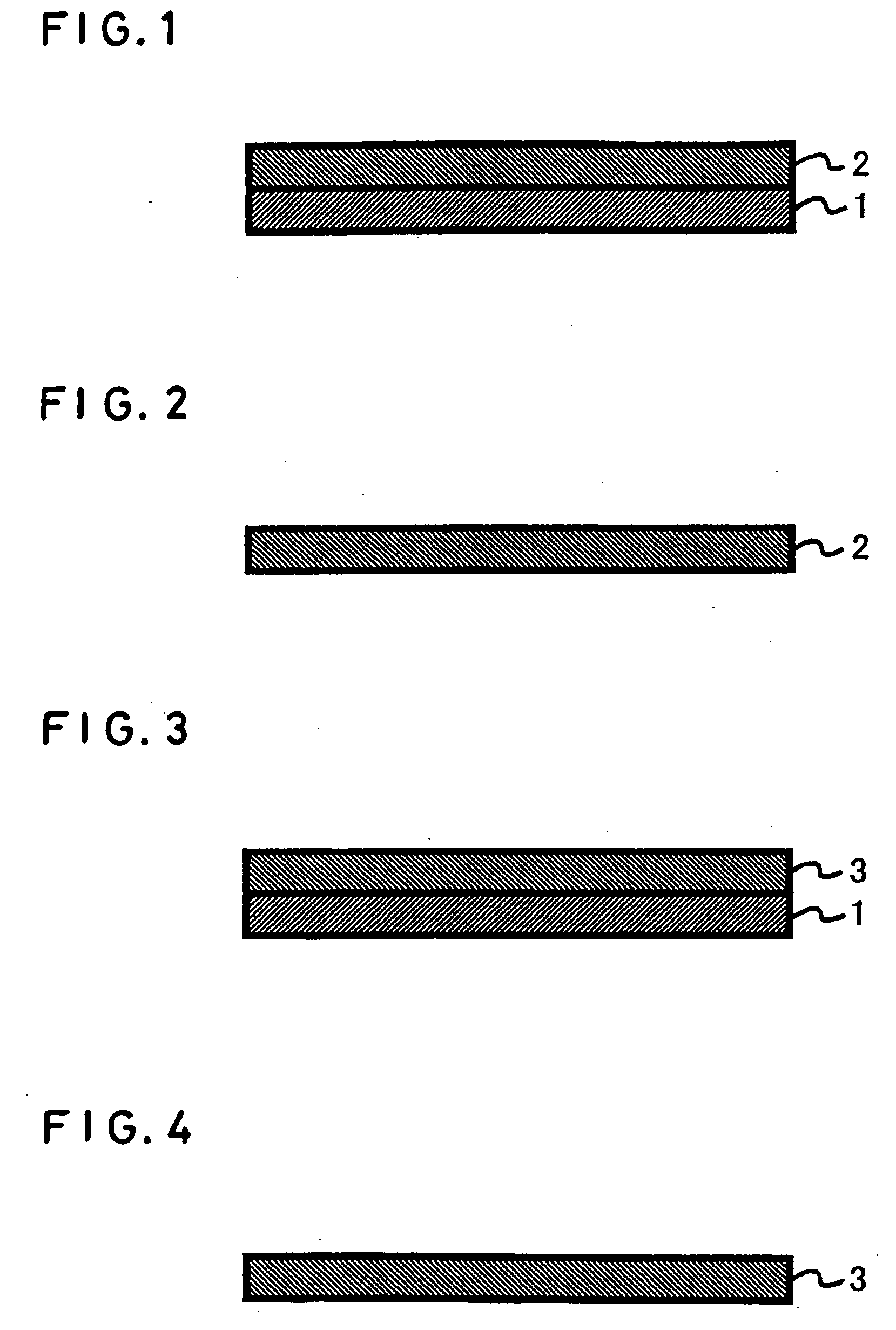
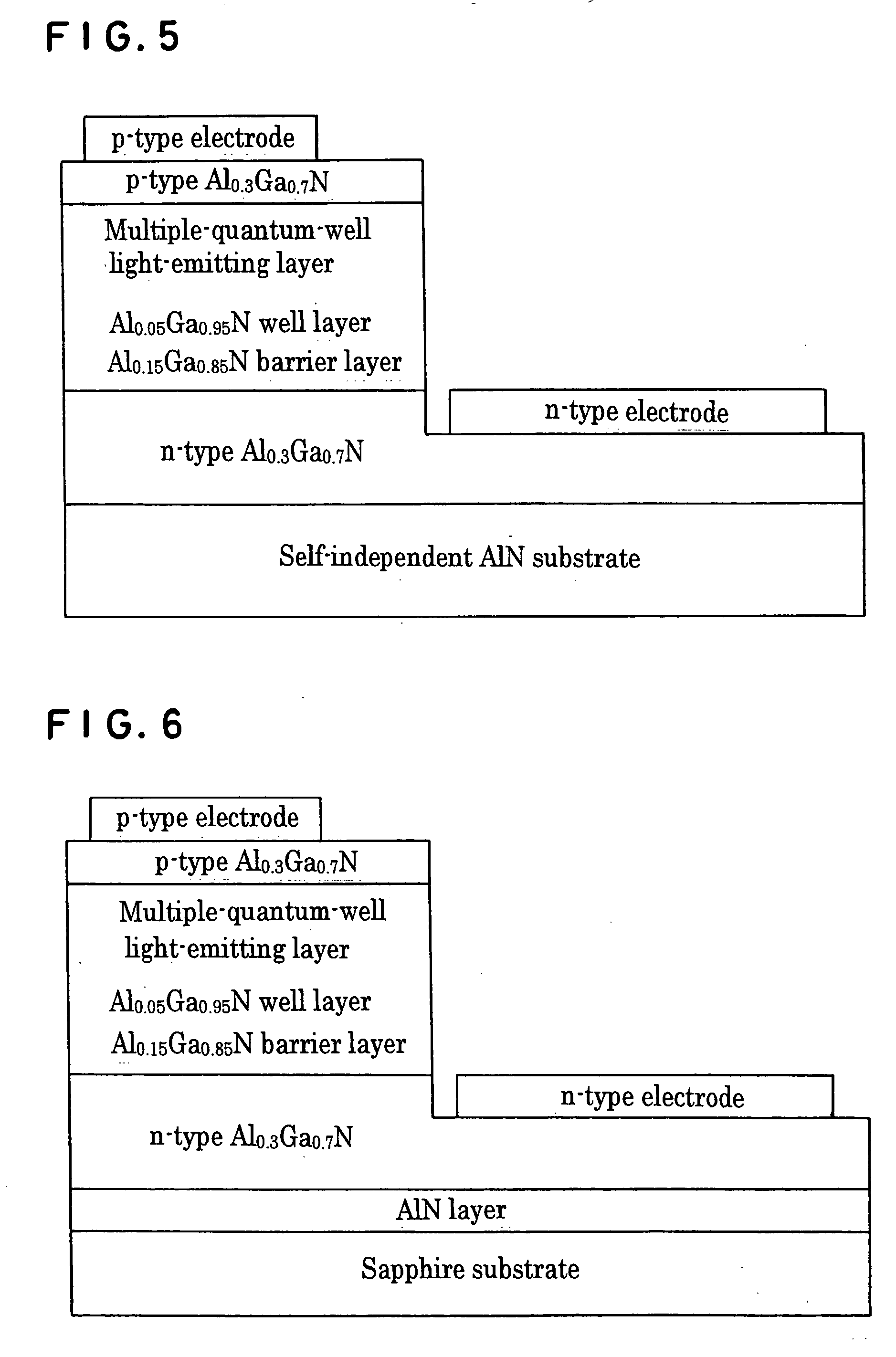
[0045]FIG. 1 is a cross section typically showing a structure having an layer of AlN deposited on a sapphire substrate, and FIG. 2 is a cross section showing the AlN layer having exfoliated from the sapphire substrate.

[0046] A structure having an AlN layer deposited on a sapphire substrate was produced in accordance with the following procedure using the ordinary pressure-reduced MOCVD means. First, a (0001-sapphire substrate 1 was placed on a susceptor having highly pure graphite (for a semiconductor) coated with tantalum carbide (TaC). The resultant susceptor was set in position within a vapor phase growth reaction furnace formed of stainless steel and highly pure graphite (for a semiconductor) coated with thermally decomposed carbon (PYROCARB), and nitrogen gas was circulated within the reaction furnace to purge the inside of the reaction furnace.

[0047] Once the inside of the vapor phase growth reaction furnace was evacuated, hydrogen and nitrogen were circulated with...

Example

EXAMPLE 2

[0053] In place of the AlN film of the stacked structure fabricated in Example 1, an AlxGa1-xN (01Ga1-xN (0xGa1-xN (0

[0054] The fabrication method was the same as that in Example 1 while TMA and TMG were supplied as the raw materials for four hours to fabricate an AlxGa1-xN (0

[0055] The AlxGa1-xN (03) gas was supplied into the vapor growth reaction furnace so that a V / III ratio might be 100.

[0056] The wafer taken out was partially divided to enable the divided cross section to be observed. The cross section was observed with an SEM to find that an AlN film of about 80 μm was deposited. An X-ray diffraction was used to find that the half-value widths of the diffraction peaks at the (0002) and (10-10) planes were 500 seconds and 1000 seconds, respectively, and confirm that the AlN film was a single crystal. In addition, it was confirmed from t...

Example

EXAMPLE 3

[0058] An AlN substrate was fabricated by following the procedure in Example 1 while the growth temperature in the AlN stacked structure fabricated in Example 1 was set to be 1150° C.

[0059] As a result, the half-value width of the diffraction peak at the (0002) plane by the X-ray diffraction was 2000 seconds or more. Thus, the AlN substrate was lower in crystallinity than that in Example 1.


PUM

PropertyMeasurementUnit
Temperatureaaaaaaaaaa
Speedaaaaaaaaaa
Ratioaaaaaaaaaa

Abstract

A substrate is formed of AlxGa1-xN, wherein 0<x≦1. The substrate is a single crystal and is used producing a Group III nitride semiconductor device. A method for producing a substrate of AlxGa1-xN, wherein 0<x≦1, includes the steps of forming a layer of AlxGa1-xN, wherein 0<x≦1, on a base material and removing the base material. The method adopts the MOCVD method using a raw material molar ratio of a Group V element to Group III element that is 1000 or less, a temperature of 1200° C. or more for forming the layer of AlxGa1-xN, wherein 0<x≦1. The base material is formed of one member selected from the group consisting of sapphire, SiC, Si, ZnO and Ga2O3. The substrate is used for fabricating a Group II nitride semiconductor device.

Description

BACKGROUND OF THE INVENTION [0001] 1. Field of the Invention [0002] The present invention relates to an AlGaN substrate and a production method thereof, [0003] 2. Description of the Prior Art [0004] A Group III nitride semiconductor has heretofore been utilized as a functional material for configuring Group III nitride semiconductor light-emitting devices of p-n junction structure, such as Light-Emitting Diodes (LEDs), Laser Diodes (LDs), etc., emitting visible light of short wavelength. In this case, in configuring an LED having a light-emitting layer of gallium indium nitride (Gale), for example, to enhance the quality of the light-emitting layer and emitting light of blue or green band, a layer of gallium nitride (GaN) has been formed on a substrate in a thickness of several μm (hereinafter called an “under layer”) to improve the crystallinity thereof and make it easy to extract light. When fabricating a device necessitating crystallinity of higher quality, such as an LD, a cryst...

Claims


Application Information

Patent Timeline
IPC IPC(8): C30B23/00C30B25/00C30B28/12C30B28/14
CPCC30B25/02C30B29/403H01L21/0237H01L21/0242Y10S117/915H01L21/0262H01L33/0075C03B25/02H01L21/0254
Inventor AMANO, HIROSHIBANDO, AKIRA
Owner SHOWA DENKO KK
Why Eureka
Try Eureka