Method and system for mask optimization

a mask and optimization technology, applied in the field of mask optimization, can solve the problems of high manufacturing cost and cycle time, high yield loss during the semiconductor manufacturing process, and the need to meet the shrinking feature siz

Active Publication Date: 2008-06-19
CADENCE DESIGN SYST INC
View PDF21 Cites 252 Cited by
  • Summary
  • Abstract
  • Description
  • Claims
  • Application Information

AI Technical Summary

Problems solved by technology

The demand to meet shrinking feature size is a challenge faced by the IC industry.
As more RET is required, manufacturing costs and cycle time increase exponentially.
However, a wealth of design knowledge is stripped out into this geometry-only format, and therefore is unavailable to any data file derived from it or any design or manufacturing integration process occurring thereafter.
Yield loss during the semiconductor manufacturing process is very problematic.
There are various approaches to identifying lithography critical areas to monitor on the wafer af

Method used


Image

  • Method and system for mask optimization
  • Method and system for mask optimization
  • Method and system for mask optimization

Examples


Embodiment Construction

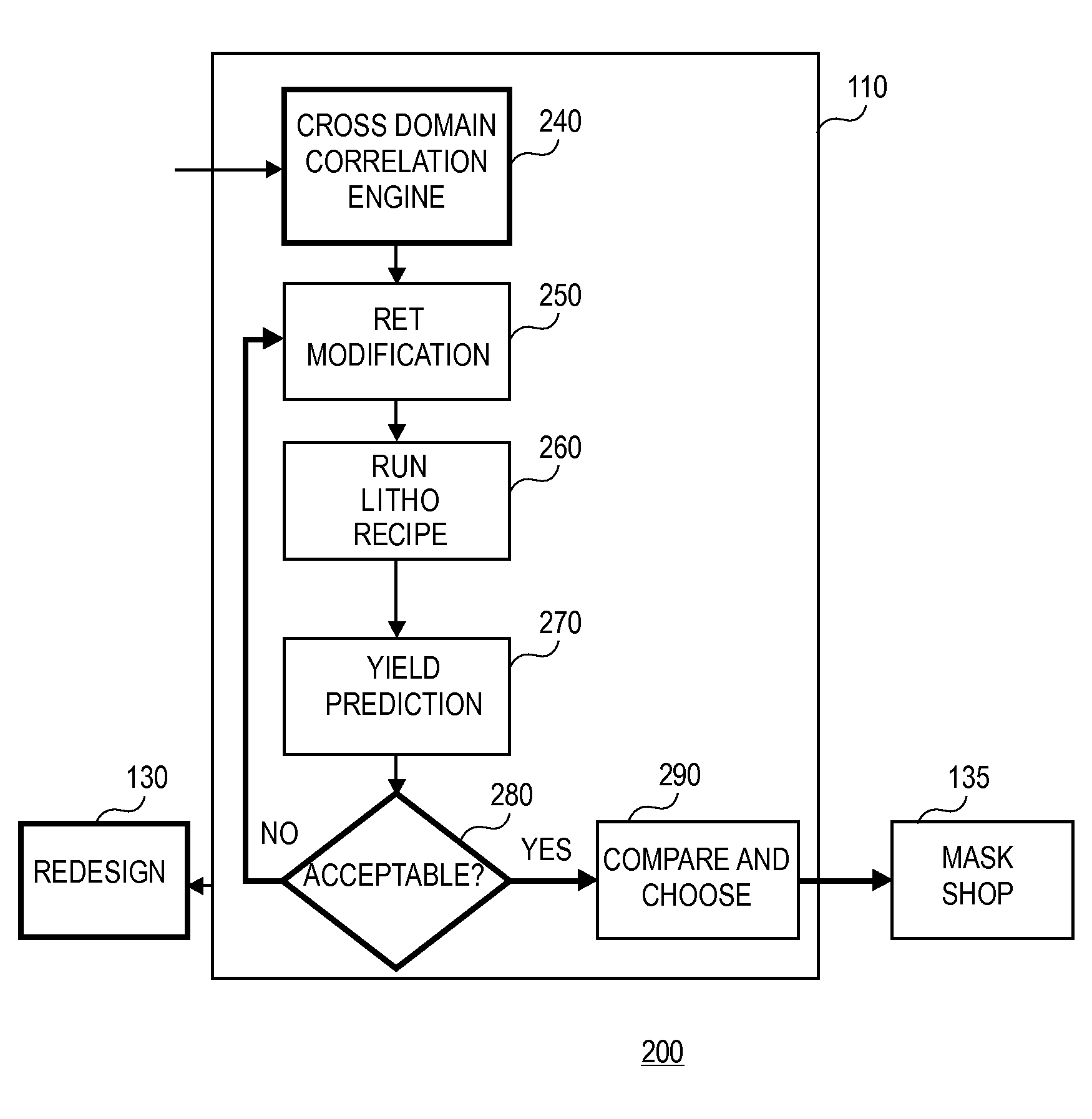
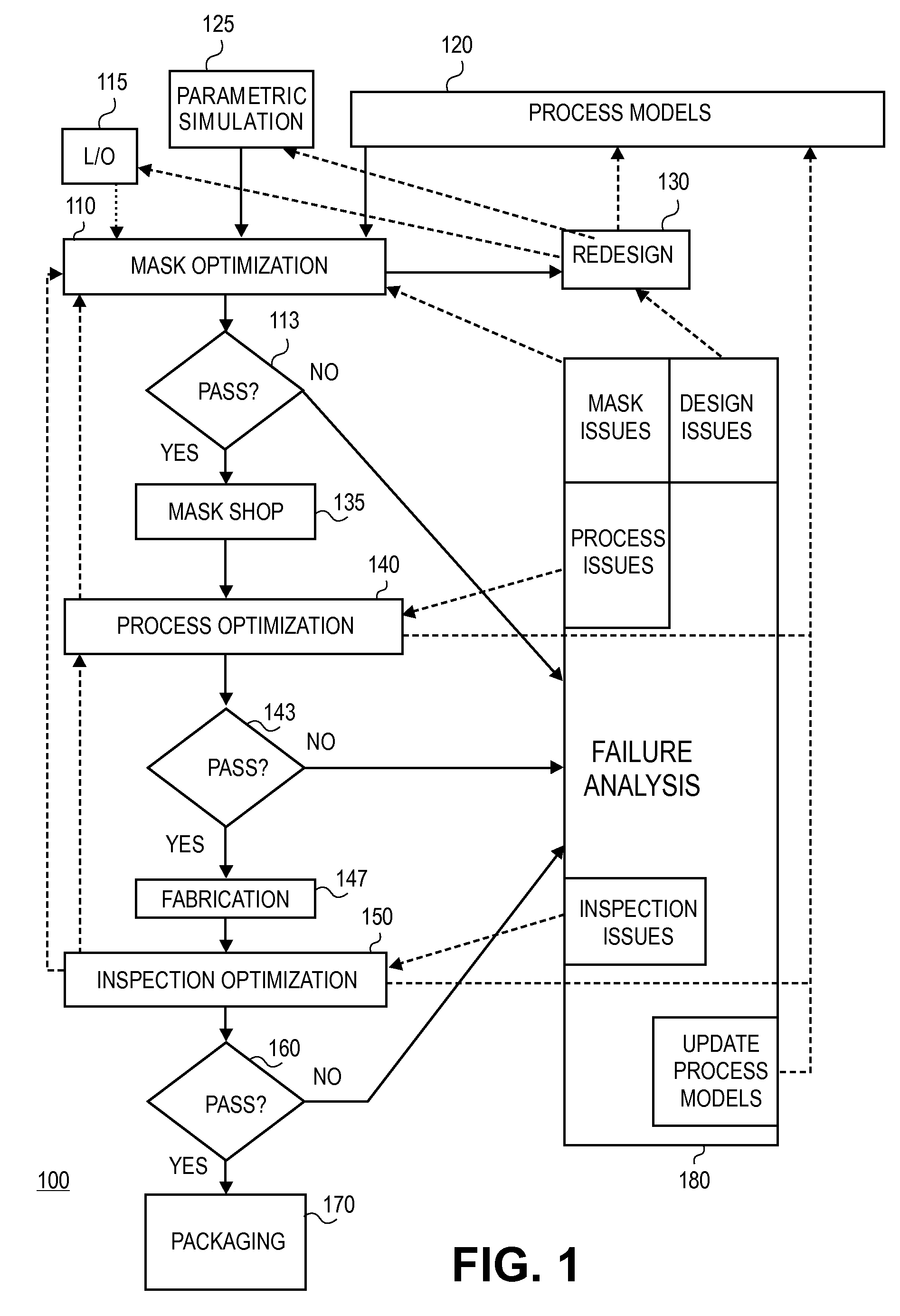
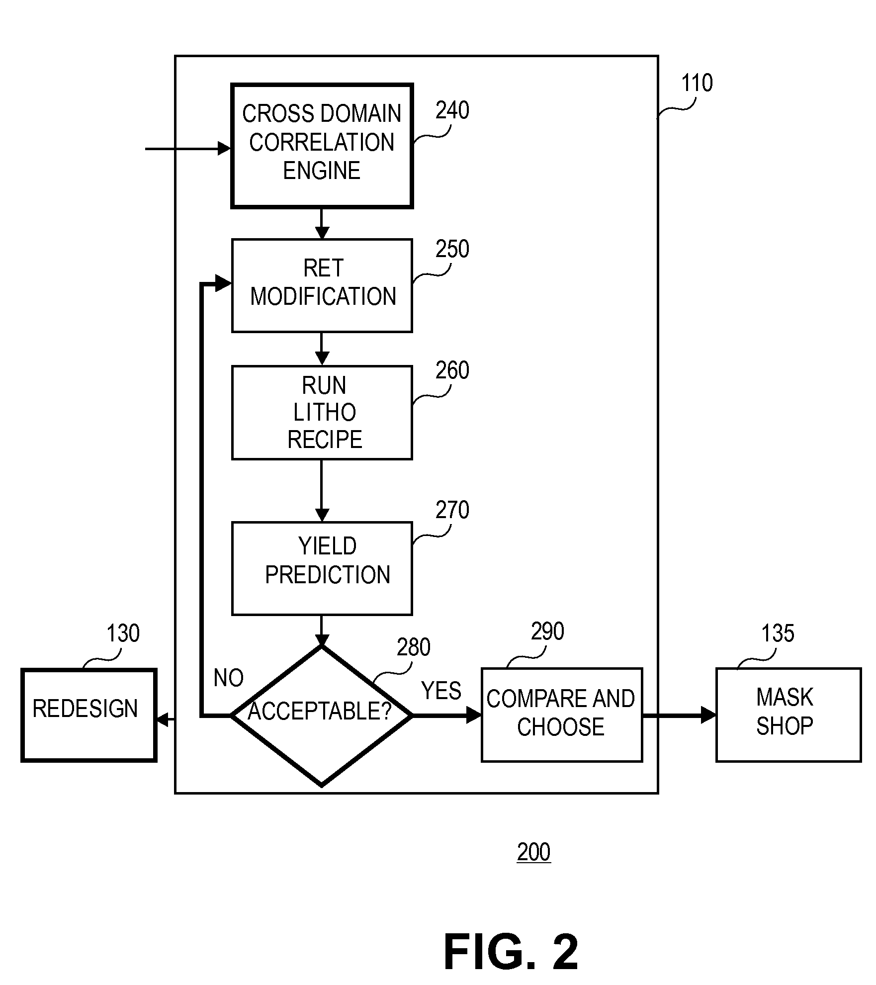
[0025]Modeling and cross correlation of design predicted criticalities for optimization of semiconductor manufacturing include using feedback loops where information from the manufacturing process is provided to a cross correlation engine for optimization of semiconductor manufacturing. In an embodiment, the information developed in manufacturing integrated circuits (ICs) is used by the designers to improve the efficiency and accuracy of future manufactured products. The information may include parametric information, functional information, and hot spots determination. The sharing of information allows for design intent to be reflected in manufacturing metrology space; thus, allowing for more efficient and intelligent metrology.

[0026]Currently, there is not much insight in the design when the ICs are being manufactured. When design files are given to manufacturing, not much continuity exist between design and manufacturing. Closing this loop brings manufacturing into design so desi...


PUM


Abstract

A method and apparatus for mask optimization is provided. Mask design and production is optimized by providing proper weighting parameters for critical features. The parameters may include information such as parametric information, functional information, and hot spots determination.

Description

FIELD OF THE INVENTION[0001]The present invention relates to design for manufacturing (DFM) for the design and production of integrated chips.BACKGROUND OF THE INVENTION[0002]The production of integrated circuits (IC) requires many different skills using knowledge from various disciplines. This process generally starts with the design of an IC chip, including the various circuit elements, their electrical interconnects, and their physical layout across the chip. The IC design typically describes each layer required to fabricate the IC in a FAB using a photolithographic process. There are generally many layers to an IC chip.[0003]The design is analyzed with respect to its physical layout. For example, wire width may be determined and efficient routing and placement of components may occur. Process model may also be used in analyzing the design. This information usually is obtained from a library provided by the manufacturers.[0004]After an integrated circuit is designed, a photomask ...

Claims


Application Information

Patent Timeline
IPC IPC(8): G06F17/50
CPCG06F17/5081G03F1/144G03F1/36G06F30/398
Inventor CHAN, KEVINDREGE, EMMANUELJAKATDAR, NICKHILLITVINTSEVA, SVETLANAMILLER, MARK A.RAQUEL, FRANCIS
Owner CADENCE DESIGN SYST INC
Why Eureka
Try Eureka