Process integration scheme to lower overall dielectric constant in BEoL interconnect structures

a process integration and overall dielectric constant technology, applied in the field of backend of line (beol) interconnect structures, can solve the problems of reducing yield, copper can deleteriously diffuse from the via into the dielectric material, and failure to connect to conductive lines

Inactive Publication Date: 2008-06-26
LAM RES CORP
View PDF20 Cites 40 Cited by
  • Summary
  • Abstract
  • Description
  • Claims
  • Application Information

AI Technical Summary

Benefits of technology

[0018]Still another exemplary method of fabricating an interconnect structure comprises forming a first conductive line in a dielectric layer, forming a first capping layer selectively over the first conductive line, and forming a low-k layer over the first capping layer and in contact with the dielectric layer. The method further comprises exposing the conductive line including forming a mask layer having an opening over the low-k layer, narrowing the opening in the mask layer, and forming a via by extending the narrowed opening through the low-k layer and at least to the first capping layer. The method further comprises forming a first diffusion barrier layer on sidewalls of the via, and filling the via with a first conductive material. In some embodiments, extending the narrowed opening at least to the first capping layer includes extending the narrowed opening through the first capping layer and to the first conductive line. Forming the first conductive line in the dielectric layer can include forming a second diffusion barrier layer in the dielectric layer. The method can also comprise forming a second conductive line in the low-k layer. In some of these embodiments, the method can further comprise forming a second capping layer selectively over the second conductive line.

Problems solved by technology

One problem that is encountered as the conductive lines within BEoL interconnect structures are made more narrow pertains to the positioning of vias relative to those conductive lines.
However, if vias and conductive lines are sufficiently misaligned, vias will land on the dielectric material between the conductive lines and therefore fail to connect to conductive lines.
If a via lands partially on a conductive line, and partially on the dielectric material, although an electrical connection is made between the conductive line and the via, copper can deleteriously diffuse from the via into the dielectric material.
Additionally, the reduced area of the electrical connection becomes an area of higher current density which accelerates void formation in the via and can lead to failures and reduced yields.
Some of these dielectric layers, though thin, are characterized by undesirably large dielectric constants that raise the overall dielectric constant.

Method used


Image

  • Process integration scheme to lower overall dielectric constant in BEoL interconnect structures
  • Process integration scheme to lower overall dielectric constant in BEoL interconnect structures
  • Process integration scheme to lower overall dielectric constant in BEoL interconnect structures

Examples


Embodiment Construction

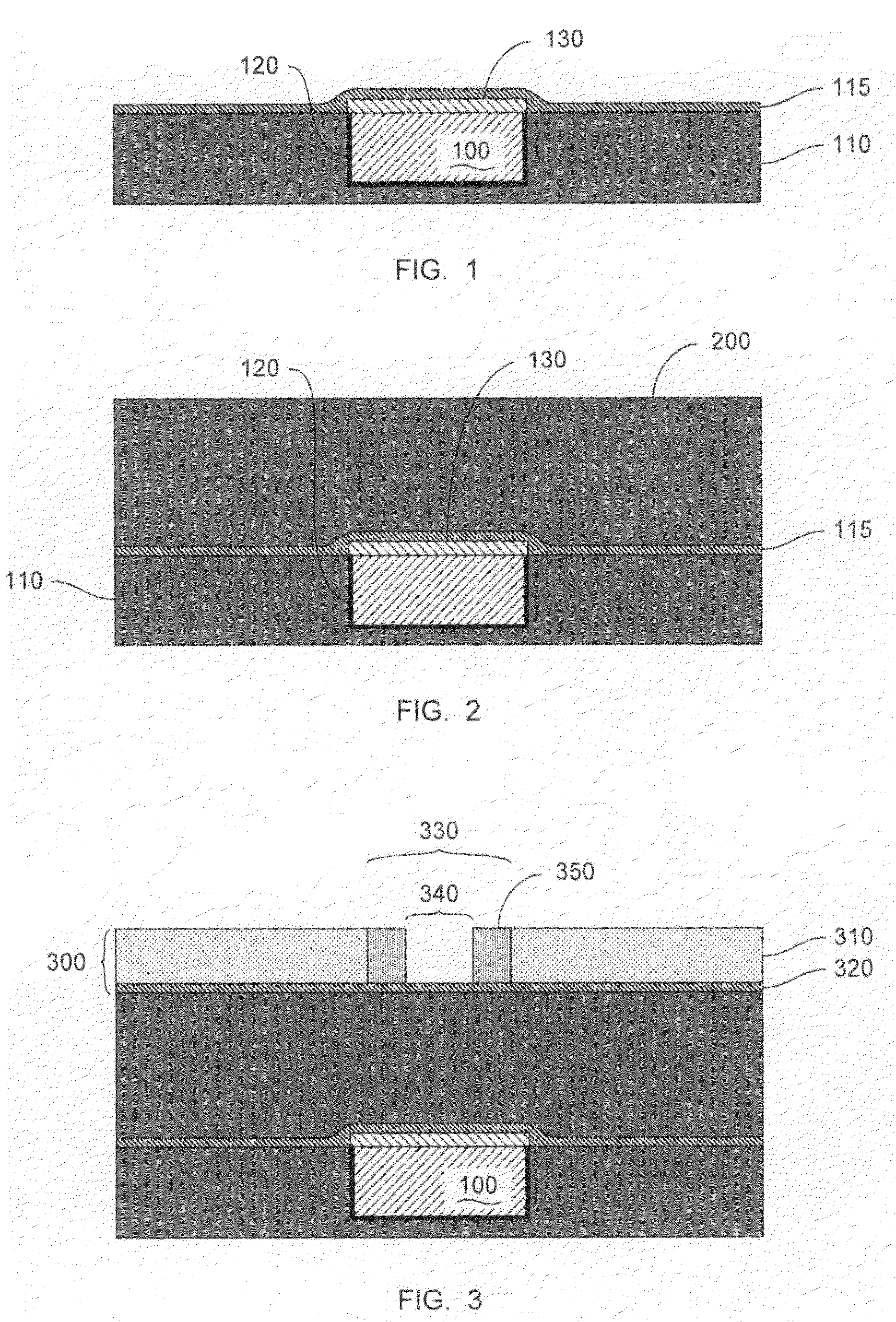
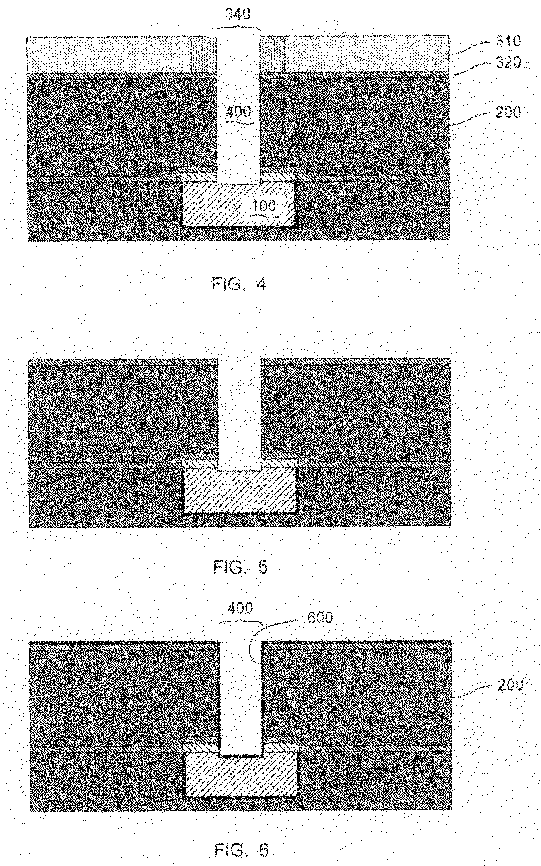
[0023]The present invention provides methods for forming Back-End of Line (BEoL) interconnect structures characterized by reduced overall dielectric constant values. Reductions in the dielectric constant are achieved, for example, through the elimination of dielectric barrier layers with high dielectric constants and / or the substitution of thinner diffusion barrier layers. The methods of the invention employ conformal diffusion barrier layers and selectively formed capping layers to isolate conductive lines and vias from surrounding dielectric layers. The methods of the invention also employ techniques to narrow openings in photoresist masks to define narrower vias. Employing more narrow vias increases the amount of misalignment that can be tolerated in the registration of the masks used to form the openings. The increased tolerance allows, in turn, for narrower conductive lines and thus for increased routing densities.

[0024]FIG. 1 provides a cross-sectional view of a conductive lin...


PUM


Abstract

Back-End of Line (BEoL) interconnect structures, and methods for their manufacture, are provided. The structures are characterized by narrower conductive lines and reduced overall dielectric constant values. Conformal diffusion barrier layers, and selectively formed capping layers, are used to isolate the conductive lines and vias from surrounding dielectric layers in the interconnect structures. The methods of the invention employ techniques to narrow the openings in photoresist masks in order to define narrower vias. More narrow vias increase the amount of misalignment that can be tolerated between the vias and the conductive lines.

Description

CROSS-REFERENCE TO RELATED APPLICATIONS[0001]This application claims the benefit of U.S. Provisional Patent Application No. 60 / 887,279 filed on Dec. 26, 2006 and entitled “Process Integration Scheme to Lower Overall Dielectric Constant in BEoL Interconnect Structures” which is incorporated herein by reference.BACKGROUND OF THE INVENTION[0002]1. Field of the Invention[0003]The present invention relates generally to the field of semiconductor devices and more particularly to Back-End of Line (BEoL) interconnect structures and methods for their fabrication.[0004]2. Description of the Prior Art[0005]Increased semiconductor device performance can be achieved, at least in part, through the further miniaturization of features such as transistors. Decreased feature sizes, and decreased spacings between features, allow more features to be placed in a unit area for greater device performance. Back-End of Line (BEoL) interconnect structures include conductive lines that connect to the features...

Claims


Application Information

Patent Timeline
Patent Type & Authority Applications(United States)
IPC IPC(8): H01L21/4763H01L23/52
CPCH01L21/76805H01L21/76807H01L21/76816H01L21/76822H01L21/76843H01L2924/0002H01L21/76846H01L21/76849H01L2924/00H01L21/3205H01L21/4763H01L21/768H01L23/48
Inventor BRIGHT, NICOLASHEMKER, DAVIDREDEKER, FRITZ C.DORDI, YEZDI
Owner LAM RES CORP
Why Eureka
Try Eureka