Cluster tool and method for process integration in manufacture of a gate structure of a field effect transistor

a technology of field effect transistor and gate structure, which is applied in the direction of measurement devices, semiconductor/solid-state device testing/measurement, instruments, etc., can solve the problems of reducing the productivity of field effect transistor manufacturing, increasing the risk of contamination, and damaging the gate structure being fabricated

Inactive Publication Date: 2007-02-01
APPLIED MATERIALS INC
View PDF33 Cites 32 Cited by
  • Summary
  • Abstract
  • Description
  • Claims
  • Application Information

AI Technical Summary

Problems solved by technology

In non-vacuumed environment, the substrates are exposed to mechanical and chemical contaminants, such as particles, traces of gaseous halogen-based reactants, and the like, that may damage the gate structures being fabricated.
As gate structures become smaller and / or thinner to increase the device speed, the risk of contamination becomes increased.
Additionally, the time spent on transferring the substrate between the processing reactors and between the processing reactors and metrology tools decreases productivity in manufacture of the field effect transistors.

Method used


Image

  • Cluster tool and method for process integration in manufacture of a gate structure of a field effect transistor
  • Cluster tool and method for process integration in manufacture of a gate structure of a field effect transistor
  • Cluster tool and method for process integration in manufacture of a gate structure of a field effect transistor

Examples


Embodiment Construction

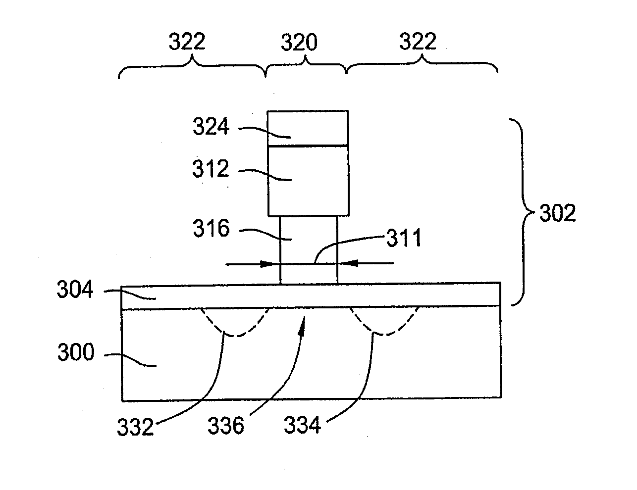
[0021] The present invention is a cluster tool and method for process integration in manufacture of a gate structure of a field effect transistor having a high-k gate dielectric, such as a complementary metal-oxide-semiconductor (CMOS) field effect transistor, and the like. The invention may be used for fabricating ultra-large-scale integrated (ULSI) semiconductor devices and circuits.

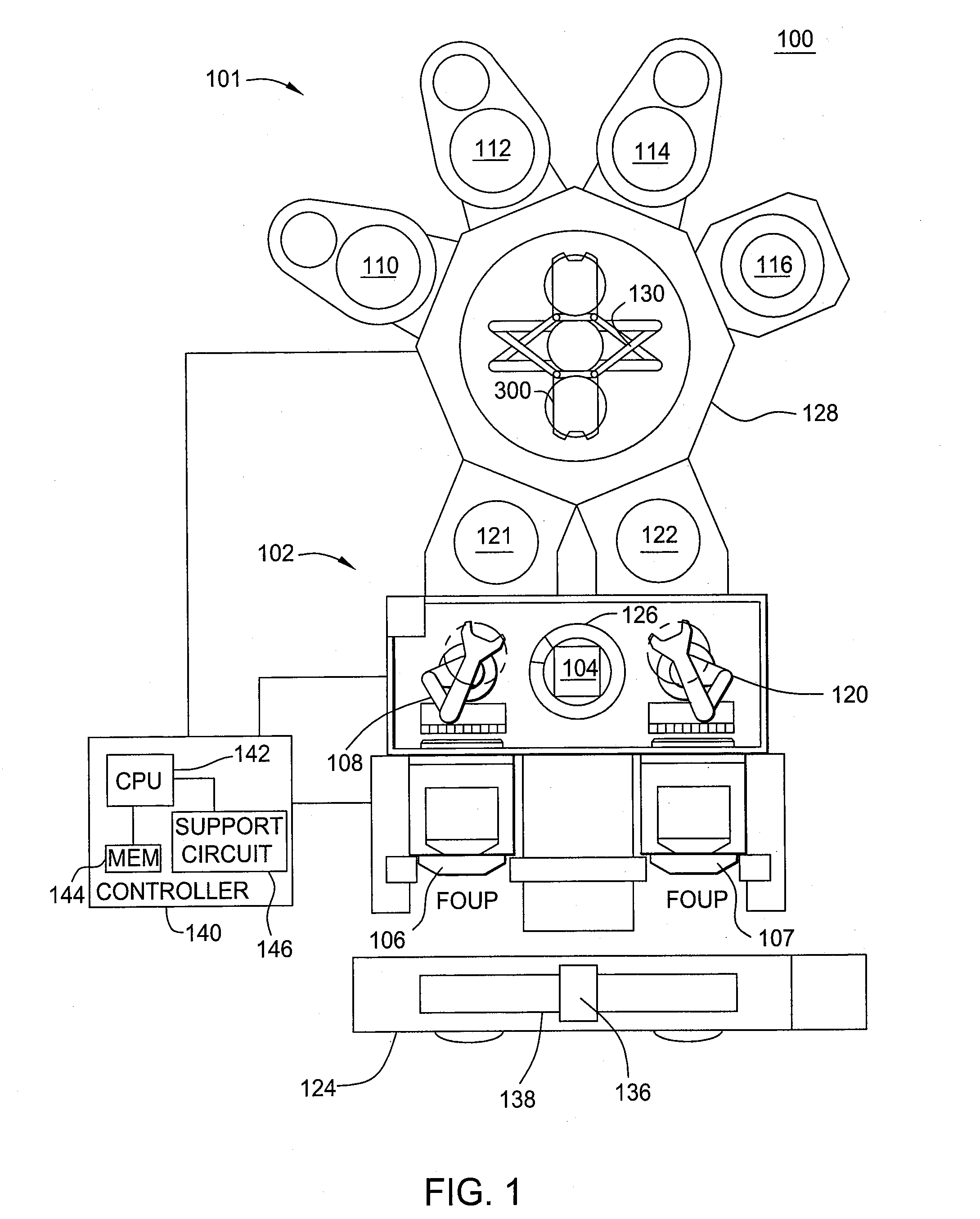
[0022]FIG. 1 depicts a schematic diagram of an exemplary integrated semiconductor substrate processing system (e.g., cluster tool) 100 of the kind used in one embodiment of the invention.

[0023] The system 100 illustratively includes a vacuum-tight processing platform 101, an input / output module 102, and a system controller 140. In one embodiment, the platform 101 comprises processing modules 110, 112, 114 and 116 and at least one load-lock chamber (load-lock chambers 121 and 122 are shown), which are coupled to a common vacuumed substrate transfer chamber 128.

[0024] The load-lock chambers 121 and 12...


PUM


Abstract

A method and apparatus for process integration in manufacture of a gate structure of a field effect transistor are disclosed. The method includes assembling an integrated substrate processing system having a metrology module and a vacuumed processing platform to perform controlled and adaptive plasma processes without exposing the substrate to a non-vacuumed environment.

Description

CROSS-REFERENCE TO RELATED APPLICATIONS [0001] This application is a divisional of co-pending U.S. patent application Ser. No. 10 / 909,009, filed Jul. 29, 2004, which is herein incorporated by reference.BACKGROUND OF THE INVENTION [0002] 1. Field of the Invention [0003] The present invention generally relates to a cluster tool and method of fabricating devices on semiconductor substrates. More specifically, the present invention relates to a cluster tool and method for process integration in manufacture of field effect transistors. [0004] 2. Description of the Related Art [0005] Integrated circuits may include more than one million micro-electronic field effect transistors (e.g., complementary metal-oxide-semiconductor (CMOS) field effect transistors) that are formed on a substrate (e.g., semiconductor wafer) and cooperate to perform various functions within the circuit. A CMOS transistor comprises a gate structure disposed between source and drain regions that are formed in the subs...

Claims


Application Information

Patent Timeline
Patent Type & Authority Applications(United States)
IPC IPC(8): H01L21/66H01L21/302
CPCH01L21/02071H01L21/31116H01L21/31122H01L21/31138H01L21/67253H01L21/32137H01L21/32139H01L21/67167H01L21/32136
Inventor KUMAR, AJAYKRISHNAMURTHY, RAMESH
Owner APPLIED MATERIALS INC
Why Eureka
Try Eureka