Capacitance sensing structure

a capacitance sensing and capacitor technology, applied in the direction of acceleration measurement in multiple dimensions, resistance/reactance/impedence, instruments, etc., can solve the problems of capacitance sensing circuit, complex and precise capacitance sensing circuit, unrecoverable functional damage, etc., to achieve enhanced sensing structure performance, spatial arrangement can be effectively saved, and the area of the sensing capacitor may be broadened.

Inactive Publication Date: 2008-06-26
DELTA ELECTRONICS INC
View PDF9 Cites 18 Cited by
  • Summary
  • Abstract
  • Description
  • Claims
  • Application Information

AI Technical Summary

Benefits of technology

[0015]As mentioned above, the capacitance sensing structure of the invention is formed between the sensing electrode layer and the conductive layers of the conductive body by the CMOS manufacturing process in conjunction with the processes of forming the suspended micro-structure. The sensing electrode layer and the conductive layers are disposed corresponding to each other, and therefore the area of the sensing capacitor may be broadened. The sensing electrode layer may be disposed on the substrate or formed in the substrate. Compared with the prior art, the test electrode and the mechanical limit stop can be integrated at different heights and therefore, the spatial arrangement can be effectively saved, the performance of the sensing structure can be enhanced, the process complexity and the manufacturing cost can be reduced, and the resolution of the capacitance variation can be further increased.

Problems solved by technology

Thus, the capacitance variation is smaller and may be hidden in the parasitical capacitance, thereby decreasing the sensing sensitivity.
Consequently, a capacitance sensing circuit, which is complicated and precise, has to be adopted to detect the capacitance variation.
In addition, since the conventional structure does not provide a test electrode and a mechanical limit stop, the sensing structure has to be operated and tested carefully after being manufactured.
When the exceeding acceleration variation is inputted, the sensing structures contact each other to form the short-circuited condition, and the unrecoverable functional damage may be caused.
If the test electrode has to be disposed additionally, the manufacturing process and cost for the test electrode are needed and the circuit layout becomes more complicated.

Method used


Image

  • Capacitance sensing structure
  • Capacitance sensing structure
  • Capacitance sensing structure

Examples


Embodiment Construction

[0025]The present invention will be apparent from the following detailed description, which proceeds with reference to the accompanying drawings, wherein the same references relate to the same elements.

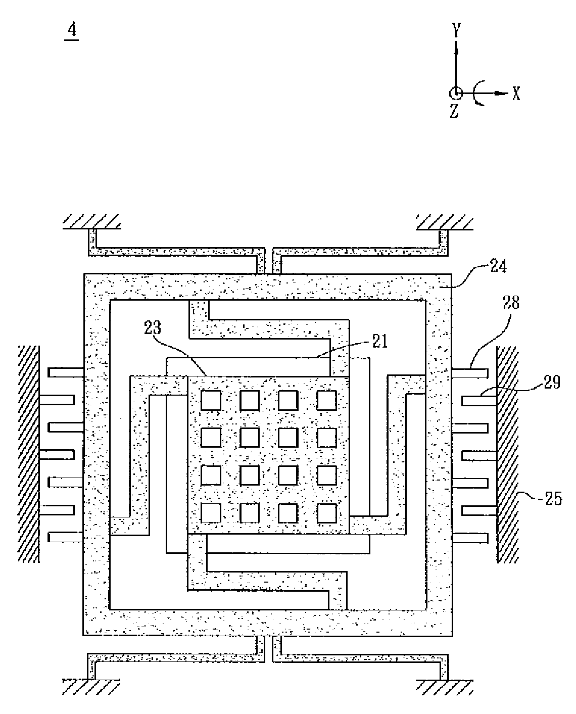
[0026]Referring to FIGS. 3 to 7, a capacitance sensing structure 2 according to an embodiment of the invention includes a substrate 20, a sensing electrode layer 21 and a conductive body 23. In this embodiment, the capacitance sensing structure 2 is manufactured by the CMOS manufacturing technology and may serve as an accelerometer, or be applied to a gyroscope or a MEMS. Herein, the capacitance sensing structure 2 serves as, for example but not limited to, the accelerometer.

[0027]The sensing electrode layer 21 is disposed on the substrate 20 (see FIGS. 4 and 5) by the CMOS manufacturing process. The substrate 20 may be a silicon (e.g., polysilicon) substrate, a silicon on glass (SOG) substrate or a glass substrate. The sensing electrode layer 21 may be made of polysilicon, metal sili...


PUM


Abstract

A capacitance sensing structure includes a substrate, a sensing electrode layer, at least one stack layer and a conductive body. The sensing electrode layer is formed on or in the substrate. The stack layer is formed on the sensing electrode layer. The conductive body is disposed over and corresponding to the sensing electrode layer and the stack layer.

Description

CROSS REFERENCE TO RELATED APPLICATIONS[0001]This Non-provisional application claims priority under 35 U.S.C. §119(a) on Patent Application No(s). 095148390 filed in Taiwan, Republic of China on Dec. 22, 2006, the entire contents of which are hereby incorporated by reference.BACKGROUND OF THE INVENTION[0002]1. Field of Invention[0003]The invention relates to a sensing structure, and in particular, to a capacitance sensing structure.[0004]2. Related Art[0005]With the enhancement of the semiconductor manufacturing technology, micro-electromechanical devices applied to a micro-electromechanical system (MEMS) are commonly manufactured using the complementary metal-oxide semiconductor (CMOS) technology.[0006]The micro-electromechanical device manufactured according to the prior art has a suspended conductive structure serving as a sensing unit, which receives an external action to move the suspended conductive structure relative to a fixed conductive structure. A variation between the su...

Claims


Application Information

Patent Timeline
Patent Type & Authority Applications(United States)
IPC IPC(8): G01R27/26
CPCG01C19/5755G01P15/18G01P15/125G01C19/5769
Inventor WANG, HORNG-JOUHSIEH, HSIEH-SHENLIANG, CHAO-JUILEE, CHENG-CHANGWANG, CHAO-QINGYUAN, ZONG-TINGCHEN, HUANG-KUNSHING, TAI-KANG
Owner DELTA ELECTRONICS INC
Why Eureka
Try Eureka