Inspection method, inspection apparatus and computer-readable storage medium storing program

a technology of inspection apparatus and computer, which is applied in the direction of measurement devices, semiconductor/solid-state device testing/measurement, instruments, etc., can solve the problems of hardly flowing electrical signals, failure to appropriately perform inspection, and breakage of probes and electronic circuits, so as to improve the reliability of inspection of electrical properties, high electrical conductivity, and stable obtained

Inactive Publication Date: 2008-06-26
TOKYO ELECTRON LTD
View PDF4 Cites 8 Cited by
  • Summary
  • Abstract
  • Description
  • Claims
  • Application Information

AI Technical Summary

Benefits of technology

[0007]According to the inspection method using the above-described fritting, even when the probes are brought into contact with the electrode on the wafer with a low load, a good electrical conduction can be obtained between the probes and the electrode, and it is demanded to stably obtain good conduction between the probes and the electrode, for example, in order to further increase the reliability of inspection of the electrical property of the wafer.
[0008]The present invention has been developed in consideration of the above points and its object is to more stably obtain the electrical conduction between probes and an object to be inspected in inspection of the electrical property of the object to be inspected such as a wafer.
[0010]The inventors verified that bias in electrical conductivity between at least one of the probe pair and the object to be inspected occurs between the anode side and the cathode side of the probe pair between which a voltage is applied during fritting. According to the present invention, polarities of the voltage applied between the probe pair are alternately changed, whereby the bias in electrical conductivity between the anode side and the cathode side of the probe pair is resolved, resulting in high conductivity between both electrodes of the probe pair. As a result, high conductivity between the probe pair and the object to be inspected can be stably obtained.
[0016]According to the present invention, high electrical conductivity between at least one of the probe pair and the object to be inspected can be stably obtained to improve the reliability of inspection of the electrical property.

Problems solved by technology

However, if an oxide film is formed on the electrode surface on the wafer, the electrical signal hardly flows to fail to appropriately perform the inspection.
In addition, strongly pressing the probes against the electrode surface to establish an electrical conduction can break the probes and the electronic circuits.

Method used


Image

  • Inspection method, inspection apparatus and computer-readable storage medium storing program
  • Inspection method, inspection apparatus and computer-readable storage medium storing program
  • Inspection method, inspection apparatus and computer-readable storage medium storing program

Examples


Embodiment Construction

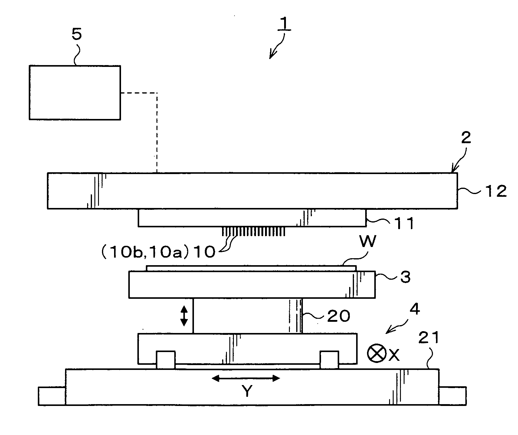
[0027]Hereinafter, a preferred embodiment of the present invention will be described. FIG. 1 is an explanatory view showing a configuration of an inspection apparatus 1 according to this embodiment.

[0028]The inspection apparatus 1 includes, for example, a probe card 2, a chuck 3 suction-holding a wafer W as an object to be inspected, a moving mechanism 4 moving the chuck 3, and a tester 5.

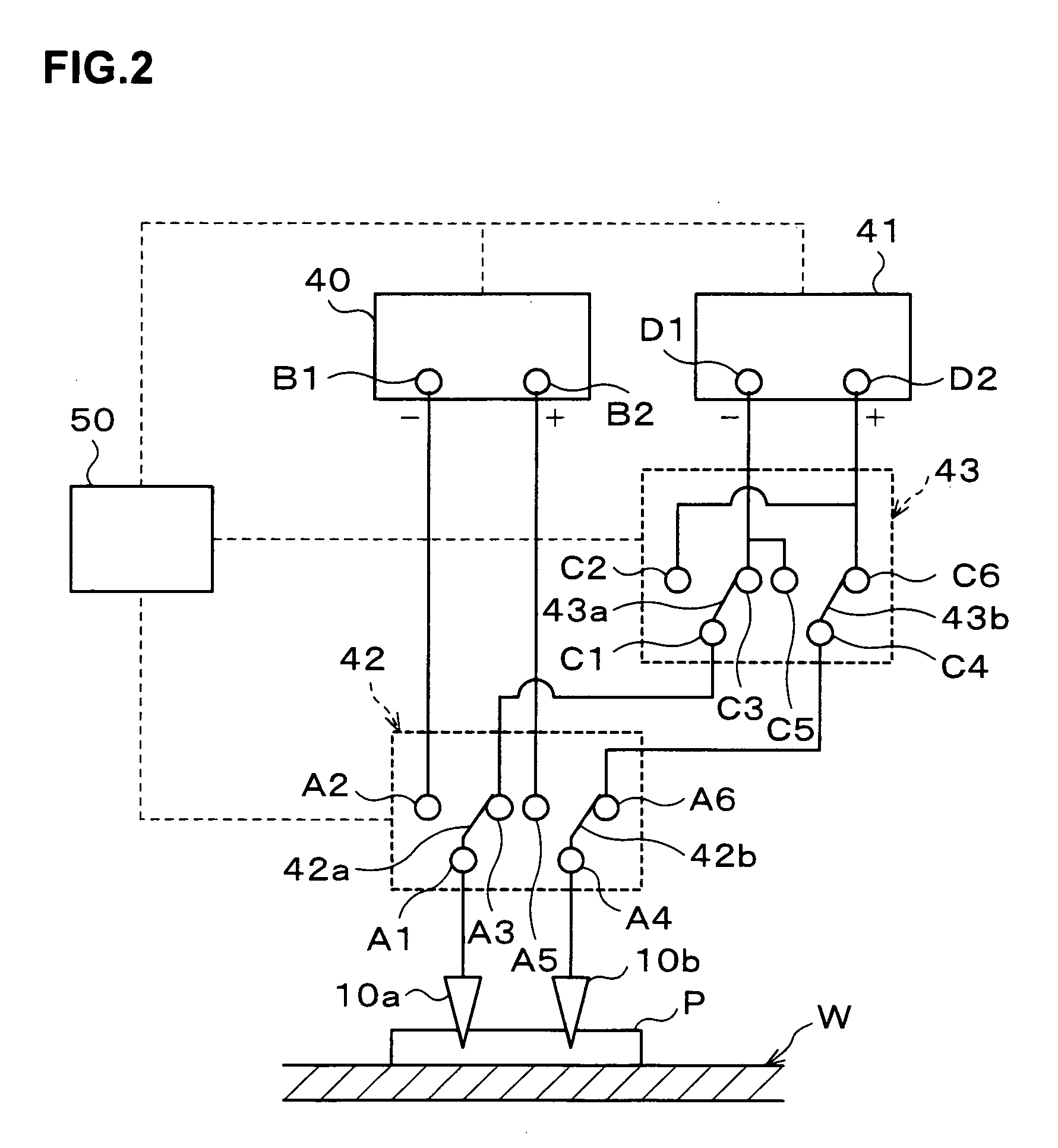
[0029]The probe card 2 includes a contactor supporting a plurality of probes 10 on its lower surface, and a printed circuit board 12 attached to the upper surface side of the contactor 11. Each of the probes 10 is electrically connected to the printed circuit board 12 via a main body of the contactor 11. To the probe card 2, the tester 5 is electrically connected so that the operation of the probe card 2 can be controlled by an electrical signal from the tester 5. The circuit configuration of the probe card 2 will be described later.

[0030]The chuck 3 is formed in an almost disk shape having a horiz...


PUM


Abstract

The present invention includes a fritting circuit applying a voltage between a probe pair composed of probes in pairs in contact with a substrate to cause a fritting phenomenon to establish an electrical conduction between at least one of the probe pair and the substrate; and a switching circuit electrically connecting the probe pair and the fritting circuit and capable of freely switching between polarities of a voltage applied between the probe pair. Voltage is applied twice between the probe pair in contact with the substrate to thereby perform fritting twice. In the two times of fritting, the polarities of the voltage applied between the probe pair are changed. According to the present invention, electrical conduction between the probes and the substrate can be obtained more stably.

Description

BACKGROUND OF THE INVENTION[0001]1. Field of the Invention[0002]The present invention relates to an inspection method of inspecting an electrical property of an object to be inspected, an inspection apparatus performing the inspection method, and a storage medium storing a program for realizing the inspection method.[0003]2. Description of the Related Art[0004]Inspection of electrical properties of electronic circuits such as IC, LSI, and the like formed, for example, on a semiconductor wafer is performed using an inspection apparatus. The inspection apparatus has a probe card electrically connected to a tester, and many probes are attached to the lower surface of the probe card. The inspection of the electronic circuits is performed by bringing, for example, the probes into contact with electrodes of the electronic circuits on the wafer and causing an electrical signal to flow to the electrodes.[0005]However, if an oxide film is formed on the electrode surface on the wafer, the ele...

Claims


Application Information

Patent Timeline
Patent Type & Authority Applications(United States)
IPC IPC(8): G01R31/02
CPCG01R31/2886G01R3/00H01L22/00
Inventor KUMAGAI, YASUNORITOH, KA
Owner TOKYO ELECTRON LTD
Why Eureka
Try Eureka