Flexible substrate integrated waveguides

a waveguide and flexible technology, applied in the direction of antennas, electrical equipment, antenna arrays, etc., can solve the problems of high loss and bad matching of feeding lines, limited system miniaturization, radiating and generating unwanted signals

Inactive Publication Date: 2008-06-26
SONY DEUT GMBH
View PDF8 Cites 104 Cited by
  • Summary
  • Abstract
  • Description
  • Claims
  • Application Information

AI Technical Summary

Problems solved by technology

These feeding lines suffer from high losses and bad matching, especially for long feeding lines in the region of mm-wave frequencies.
However, the system miniaturization is limited on one hand by the antenna size (for systems needing high gain antennas, the antenna aperture dimensions are directly proportional to the antenna gain).
Microstrip lines are simple to be integrated in the system and may require less space, but they radiate and generate unwanted signals (crosstalk).
Furthermore, they suffer from high losses, especially for mm-wave frequencies.
However, their difficulty of integration prevents them from being used in low-cost high-volume of integration.
Additionally, conventional WGs require complex transitions to integrated planar circuits; typical integration schemes are bulky and need high precision matching process which is difficult to achieve in the mm-wave frequency range.

Method used


Image

  • Flexible substrate integrated waveguides
  • Flexible substrate integrated waveguides
  • Flexible substrate integrated waveguides

Examples


Embodiment Construction

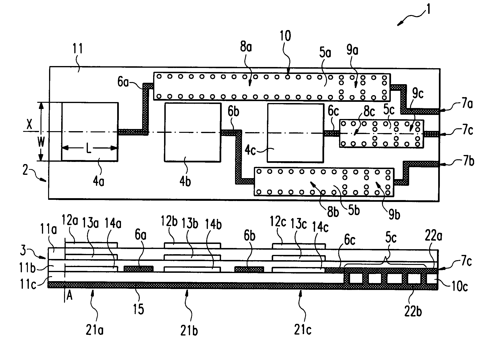
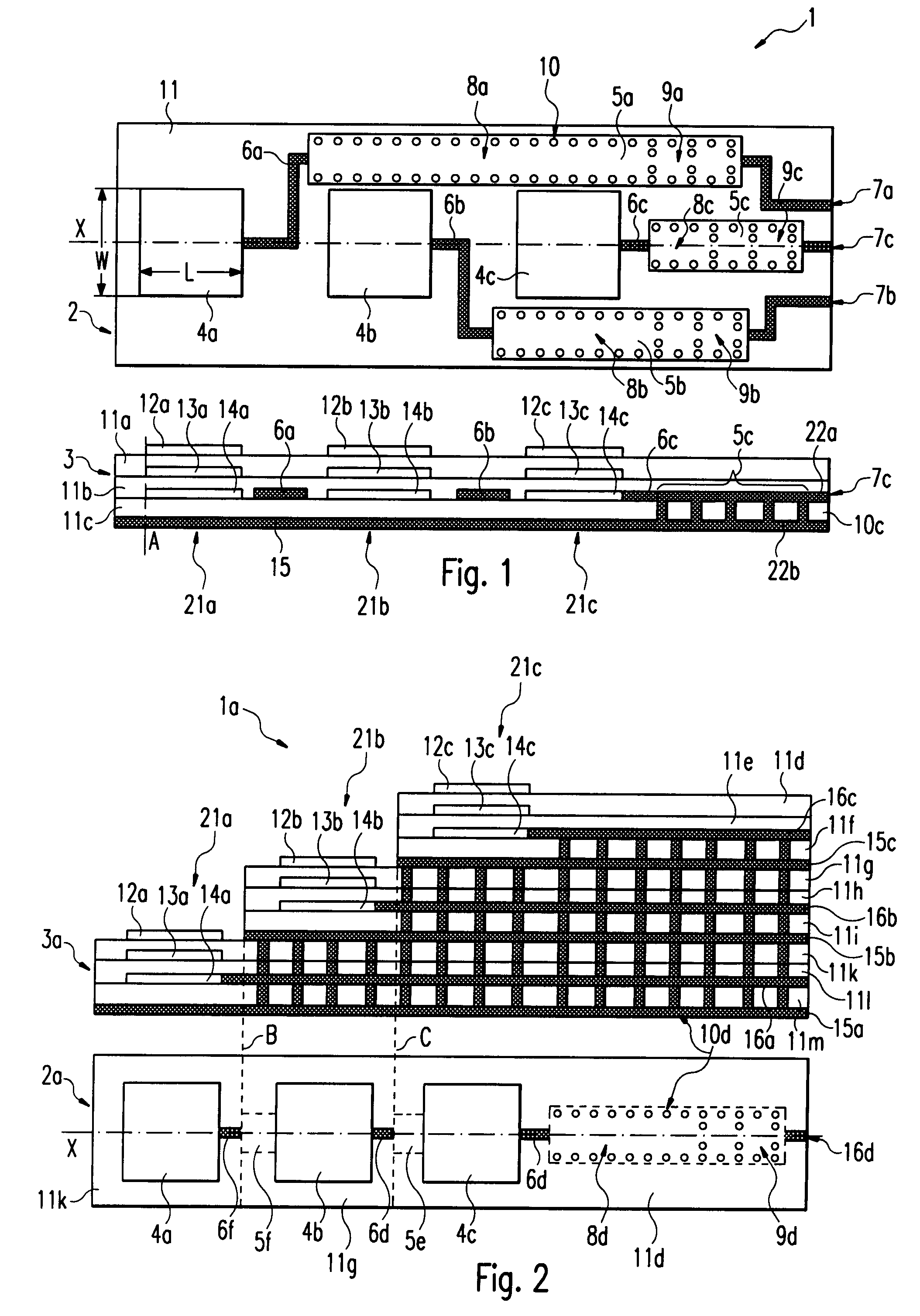
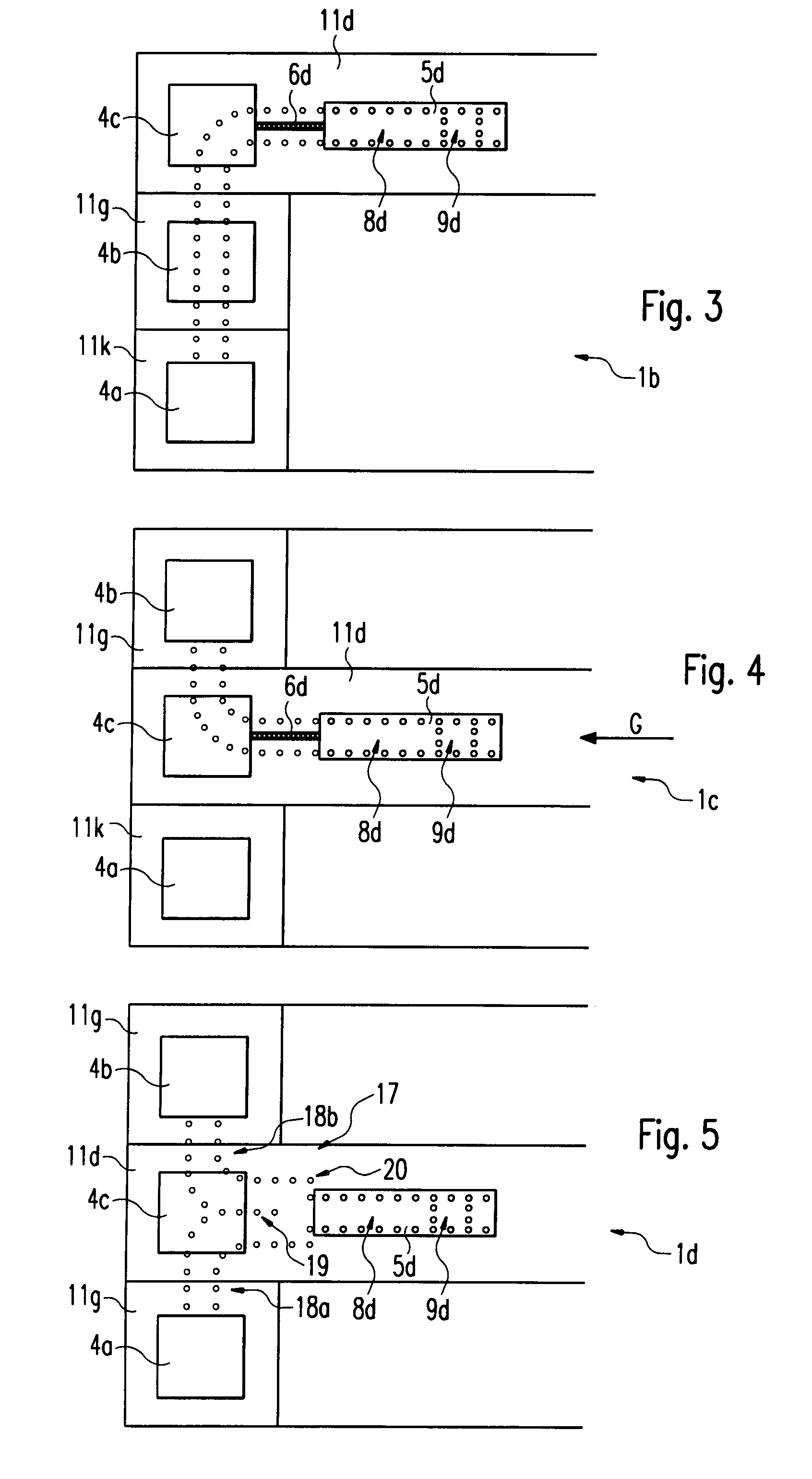
[0028]FIG. 1 shows a substrate structure (1) comprising its topview (2) and its cross section (3).

[0029]The topview (2), said topview allowing the view of the components partially lying beneath the surface, said surface comprising the top layer (11a), shows a first planar antenna (4a), a second planar antenna (4b), a third planar antenna (4c), the respective microstrip lines (6a, 6b, 6c), the respective substrate integrative waveguides (SIWG) (5a, 5b, 5c) and the respective feeding lines (7a, 7b, 7c) which are all part / integrated on or in the substrate (11). All above mentioned components are located on the same substrate / component, thus can be subsequently and / or stepwise fabricated on the same wafer or semiconductor substrate or LCP (liquid crystal polymer) substrate or any other material suitable for superimposing said substrate structure (1).

[0030]The planar antennas (4a, 4b, 4c) are located in a row and symmetrical along the symmetry axis X, are equidistant to each other and ar...


PUM


Abstract

This invention relates to a device operable to guide electromagnetic waves in substrate integrated structures, said substrate integrated structures being made in one component. In detail planar antennas are part of said substrate integrated structures, which are connected to electromagnetic waveguides. This invention also allows 3D structures of the above mentioned components in a multilayer substrate.

Description

FIELD OF INVENTION[0001]This invention relates to the field of substrate integrated structures, in particular to substrate integrated waveguides. Substrate integrated waveguides are needed particularly for high frequency signals.PROBLEM[0002]Communication systems nowadays witnessed rapid evolution towards system integration and miniaturization. The antenna and the channel filters are key components in any of these systems and the selection criteria for a communication success include among other things the antenna performance, size, weight, and cost.[0003]Multibeam antenna systems using a beam switching mechanism for the different antenna units need relatively large spaces in order to connect the antenna units to the system components. These feeding lines suffer from high losses and bad matching, especially for long feeding lines in the region of mm-wave frequencies. In addition, there is low isolation in between these lines and therefore, the crosstalk influences the filter charact...

Claims


Application Information

Patent Timeline
Patent Type & Authority Applications(United States)
IPC IPC(8): H01Q13/00
CPCH01Q21/065H01Q21/0075
Inventor KOCH, STEFANAL-TIKRITI, MAYSOUN
Owner SONY DEUT GMBH
Why Eureka
Try Eureka