Liquid crystal display with photosensor and method of fabricating the same

a technology of photosensors and liquid crystal displays, applied in semiconductor devices, instruments, electrical devices, etc., can solve problems such as power consumption increase, and achieve the effect of improving sensing efficiency

Active Publication Date: 2008-06-26
LG DISPLAY CO LTD
View PDF12 Cites 18 Cited by
  • Summary
  • Abstract
  • Description
  • Claims
  • Application Information

AI Technical Summary

Benefits of technology

[0026]An object of the present invention is to provide a liquid crystal display device including a photosensor with improved sensing efficiency, and a method of fabricating the same.

Problems solved by technology

That is, since the backlight unit emits the light of constant luminosity even in case of the relatively bright environments, it causes the increase of power consumption.

Method used


Image

  • Liquid crystal display with photosensor and method of fabricating the same
  • Liquid crystal display with photosensor and method of fabricating the same
  • Liquid crystal display with photosensor and method of fabricating the same

Examples


first embodiment

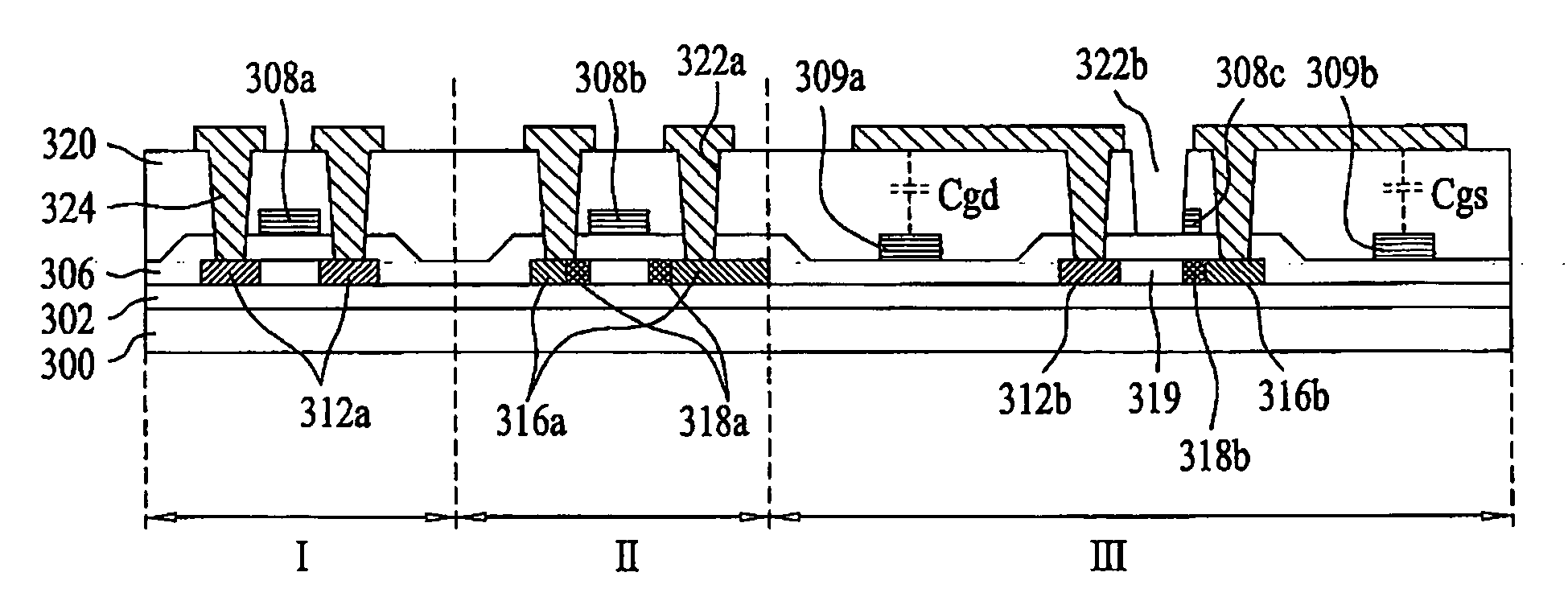
[0059]FIG. 5 is a cross section view illustrating a photosensor region and a thin film transistor region in a liquid crystal display device including a photosensor according to the present invention.

[0060]As shown in FIG. 5, a substrate 300 is defined with a first thin film transistor region (I) having a channel by a p-type ion implantation region; a second thin film transistor region (II) having a channel by an n-type ion implantation region; and a photosensor region (III).

[0061]The first thin film transistor region (I) includes a p-type semiconductor layer provided with two p-type ion implantation regions 312a on a buffer layer 302, and an ion non-implantation region formed between the two p-type ion implantation regions 312a; a gate insulation film 306 formed on the substrate 300 including the p-type semiconductor layer; a gate electrode 308a formed on the gate insulation film 306 above the ion non-implantation region; a passivation film 320 on an entire surface of the substrate ...

second embodiment

[0090]FIGS. 8A to 8C are cross section views illustrating a method of fabricating a liquid crystal display device with a photosensor according to the present invention.

[0091]First, LDD layers 318a and 318b are formed through the steps explained in FIGS. 6A and 6D according to the first embodiment of the present invention.

[0092]Subsequently, as shown in FIG. 8A, a passivation film 320 is formed on an entire surface of a substrate 300 including the LDD layers 318a and 318b, and is then patterned, thereby forming first and second contact holes 322a and 322c at the same time. At this time, the first contact hole 322a exposes semiconductor layers of source and drain regions 312a and 316a in respective first and second thin film transistor regions (I) and (II). Also, the second contact hole 322c exposes an ion implanting prevention film 308c of a photosensor region (III).

[0093]As shown in FIG. 8B, a metal film 324 is formed on the entire surface of the substrate 300 including the first an...

third embodiment

[0096]The first and second preferred embodiments of the present invention disclose that the ion implanting prevention film 308c is removed completely. The following discloses a method of fabricating a liquid crystal display device including a photosensor according to the present invention where only the central portion of the ion implanting prevention film 308c is removed.

[0097]FIGS. 9A and 9B are cross section views illustrating a method of fabricating a liquid crystal display device with a photosensor according to the third embodiment of the present invention.

[0098]First, LDD layers 318a and 318b are formed through the steps of FIGS. 6A to 6D explaining the first embodiment of the present invention.

[0099]Subsequently, as shown in FIG. 9A, a passivation film 320 is formed on an entire surface of a substrate 300 including the LDD layers 318a and 318b, and is then patterned, thereby forming first and second contact holes 322a and 322d at the same time. At this time, the first contact...


PUM

PropertyMeasurementUnit
timeaaaaaaaaaa
timeaaaaaaaaaa
weightaaaaaaaaaa

Abstract

A liquid crystal display device comprises a liquid crystal panel including first and second substrates bonded to each other with a liquid crystal layer positioned therebetween, and the photosensor, formed on the second substrate, for sensing an external light from the surroundings, wherein the photosensor includes a semiconductor layer formed on the second substrate and provided with n+-type ion implantation region, ion non-implantation region and lightly doped region; an insulation film, formed on the second substrate, for covering the semiconductor layer; a passivation film, formed on the second substrate, for covering the insulation film; a first contact hole passing through the insulation film and the passivation film, to expose source and drain regions of the semiconductor layer; source and drain electrodes connected with the source and drain regions of the semiconductor layer through the first contact hole; an ion implanting prevention film formed on the insulation film and overlapped with the ion non-implantation region; and a second contact hole passing through the passivation film and the ion implanting prevention film above the ion non-implantation region, so as to provide the external light to the ion non-implantation region.

Description

[0001]This application claims the benefit of Korean Patent Application No. P2006-132307 filed on Dec. 22, 2006, and Korean Patent Application No. P2007-098685 filed on Oct. 1, 2007, which is hereby incorporated by reference as if fully set forth herein.BACKGROUND OF THE INVENTION[0002]1. Field of the Invention[0003]The present invention relates to a liquid crystal display device, and more particularly, to a liquid crystal display device including a photosensor with improved sensing efficiency, and a method of fabricating the same.[0004]2. Discussion of the Related Art[0005]According as various mobile electronic devices, for example, mobile phone, PDA and notebook computer are developed recently, there are increasing demand for flat panel display devices with thin profile and light weight. Examples of flat panel display devices include liquid crystal display devices (LCD), field emission displays (FED), and plasma display panels (PDP). Among the flat panel display devices, the liquid...

Claims


Application Information

Patent Timeline
Patent Type & Authority Applications(United States)
IPC IPC(8): H01L31/12G02F1/133G02F1/135G02F1/1368
CPCG02F1/13318H01L27/1214G09G2360/144G02F1/1362G09G3/3406
Inventor LEE, KYUNG EONBAEK, MYOUNG KEEHWANG, HAN WOOK
Owner LG DISPLAY CO LTD
Why Eureka
Try Eureka