Passive Echo Cancellation Device And Signal Transmission Method Thereof

Active Publication Date: 2008-06-26
REALTEK SEMICON CORP
View PDF13 Cites 11 Cited by
  • Summary
  • Abstract
  • Description
  • Claims
  • Application Information

AI Technical Summary

Benefits of technology

[0008]It is therefore one of the objectives of the present invention to provide a passive echo cancellation device and a signal transceiving method thereof for a full duplex communication system. The present invention implements merely a plurality of passive elements and a simple circuit configuration to eliminate echo impairment in received signals. Also, effects of simplifying the circuit configuration, reducing the manufacturing costs and economizing power consumption can be accomplished.
[0013]using a passive echo cancellation circuit, which comprises merely passive elements, to eliminate the transmit signal contained in the echo signal according to the offset signal so as to generate an output signal containing merely signal characteristics of the receive signal.

Problems solved by technology

However, in such a system, when the network device is acquiring a signal Rx from one of the channels, a signal Tx simultaneously transmitted through the same channel may incur interference upon the received signal Rx.
As a result, the integrity of the received signal is unrecognizable and this is generally referred to as echo impairment.
Nevertheless, the implement of these active elements brings the disadvantages of relatively complex construction, higher manufacturing costs and greater power consumption to the circuits.

Method used


Image

  • Passive Echo Cancellation Device And Signal Transmission Method Thereof
  • Passive Echo Cancellation Device And Signal Transmission Method Thereof
  • Passive Echo Cancellation Device And Signal Transmission Method Thereof

Examples


first embodiment

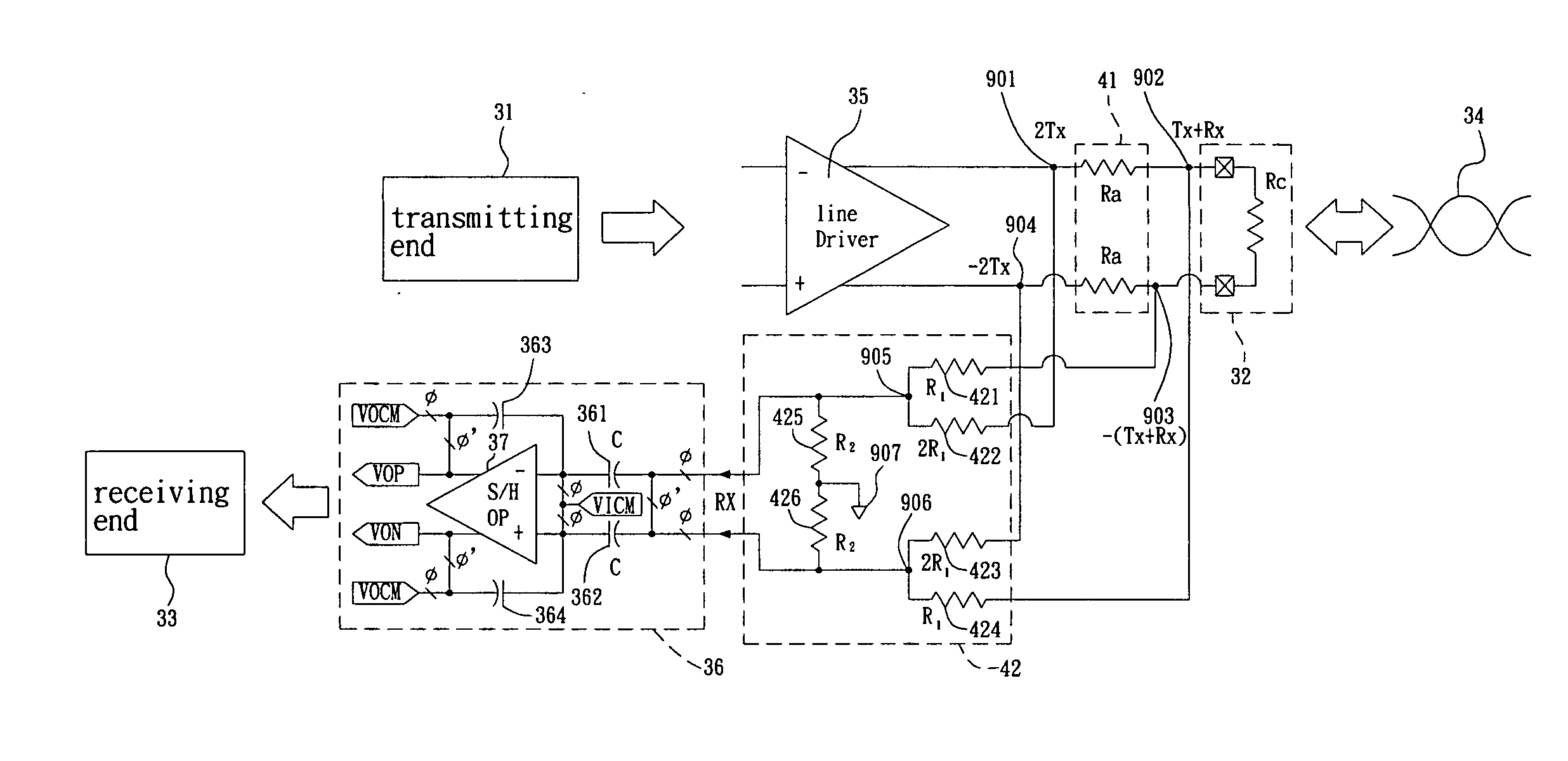
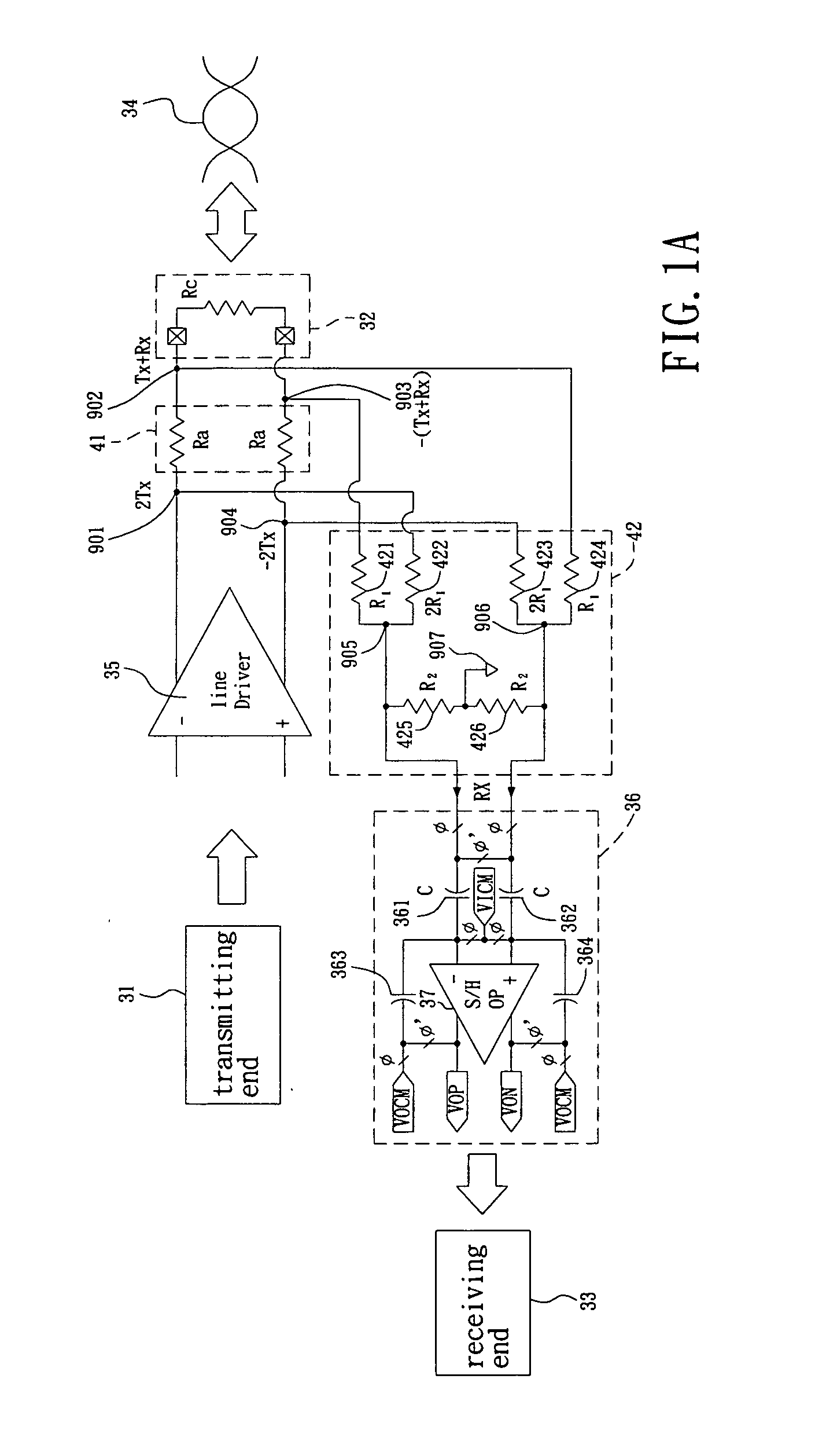
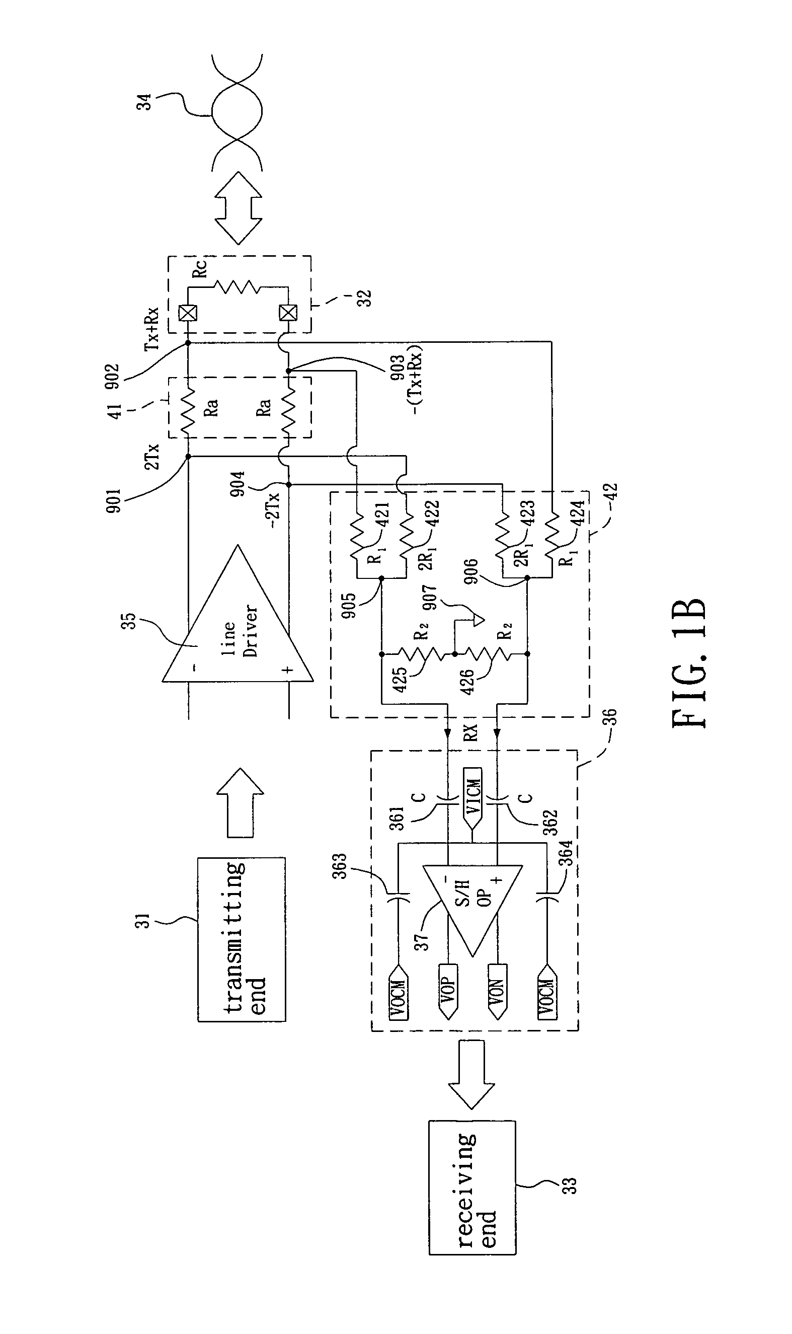
[0035]Please refer toFIGS. 1A, 1B and 1C. Therein, FIG. 1A is the circuit diagram of a passive echo cancellation device according to the present invention. FIG. 1B is another circuit diagram showing the passive echo cancellation device of FIG. 1A under a sample mode. FIG. 1C is further another circuit diagram showing the passive echo cancellation device of FIG. 1A under a hold mode.

[0036]The full duplex communication system as shown in FIGS. 1A, 1B and 1C comprises a transmitting end 31 for transmitting a transmit signal to a wiring interface 32 and a receiving end 33 for receiving a receive signal from the wiring interface 32. The transmitting end 31 may be equipped with elements including a DAC (digital-to-analog converter). The receiving end 33 may be equipped with elements including an analog front end circuit (AFE) and an ADC (analog-to-digital converter). The wiring interface 32 is provided for being connected with a twisted pair 34 and thereby further connected with another r...

second embodiment

[0049] illustrated in FIGS. 2A to 2C, the disclosed passive echo cancellation device 52 further comprises a plurality of capacitors 521˜524 (successively named as a first through a fourth capacitor), with adequate circuit connections. An input end of the first capacitor 521 is coupled with the third node 903 between the voltage-drop circuit 41 and the wiring interface 32. An input end of the second capacitor 522 is coupled with the first node 901 between the voltage-drop circuit 41 and the transmitting end 31. An input end of the third capacitor 523 is coupled with the fourth node 904 between the voltage-drop circuit 41 and the transmitting end 31. An input end of the fourth capacitor 524 is coupled with the second node 902 between the voltage-drop circuit 41 and the wiring interface 32.

[0050]For effectively eliminating the effect that the transmit signal Tx brings to the receive signal Rx, the signals 2Tx and Tx+Rx at the two ends of the voltage-drop circuit 41 are inverted and inp...

third embodiment

[0057]As shown in FIG. 3, in the passive echo cancellation device according to the present invention, a DAC provided in the transmitting end 31a can be realized through a current DAC 313 and a replica 314 of the current DAC 313. In the present embodiment, the replica 314 is substantively an offset-signal-generating circuit of the disclosed passive echo cancellation device. In other words, the replica 314 can generate an offset signal (namely a replica signal) containing only the component of the transmit signal Tx generated by the current DAC 313. Besides, the first through fourth resistors 421a˜424a of the echo cancellation circuit 42a have the same resistance value R1.

[0058]In the third embodiment, the current DAC 313 comprises a plurality of converting units 313l-313n. Each of the converting units 313l-313n is capable of conducting D / A conversion to one bit in the digital signal (D1 . . . DN) that is to be converted. For example, if the digital signal to be converted is an 8-bit ...


PUM


Abstract

The present invention refers to a passive echo cancellation device for use in a full-duplex communication system and its signal transceiving method. The full-duplex communication system comprises a transmitting end for sending a transmit signal to a wiring interface, and a receiving end for accepting a receive signal from the wiring interface. The passive echo cancellation device comprises an offset-signal-generating circuit and a passive echo cancellation circuit composed of a plurality of passive components. The offset-signal-generating circuit generates an offset signal according to the transmit signal. The passive echo cancellation circuit is serially connected between the wiring interface and the receiving end, and is connected with the offset-signal-generating circuit. The passive echo cancellation circuit receives the offset signal in such a manner that an echo signal contained in the receive signal coming from the wiring interface is cancelled by mean of the offset signal, so as to generate an output signal containing merely the signal characteristics of the receive signal.

Description

BACKGROUND OF INVENTION[0001]1. Field of the Invention[0002]The present invention relates to communication systems, and more particularly, to a passive echo cancellation device and method.[0003]2. Description of the Prior Art[0004]With the progress of technologies, more and more applications of the Internet have been developed. In view of the growing needs for the bandwidth of networking, the packet transmission speed of the extensively used Ethernet has be enhanced from the previous speed of 10 / 100 Mbps to the current speed of more than 1 Gbps.[0005]For example, in a commonly seen Gigabit Ethernet device having a transmission speed of 1 Gbps, each port thereof comprises four channels. Wherein, each channel has a transceiver for communicating with other network devices through a transmission medium such as a twisted pair cable. Further, each transceiver typically includes a transmitting end and a receiving end. The transmitting end is provided for processing data and then transmitti...

Claims


Application Information

Patent Timeline
IPC IPC(8): H04B1/56
CPCH04B3/23H04B3/03
Inventor LIN, SHIAN RUHUANG, CHUNG CHAN
Owner REALTEK SEMICON CORP
Why Eureka
Try Eureka