Methods and apparatus for multichip module packaging

a multi-chip module and packaging technology, applied in the direction of printed circuit manufacturing, cross-talk/noise/interference reduction, printed circuit aspects, etc., can solve the problems of several drawbacks of known methods and achieve the effect of improving performan

Inactive Publication Date: 2008-07-03
CUSTOM ONE DESIGN
View PDF0 Cites 23 Cited by
  • Summary
  • Abstract
  • Description
  • Claims
  • Application Information

AI Technical Summary

Benefits of technology

[0007]The present invention addresses the shortcomings of existing packaging techniques by providing multichip packaging having improved performance.

Problems solved by technology

However, these known methods suffer from several drawbacks.

Method used


Image

  • Methods and apparatus for multichip module packaging
  • Methods and apparatus for multichip module packaging
  • Methods and apparatus for multichip module packaging

Examples


Embodiment Construction

[0029]The present invention addresses the shortcomings of prior art MCMs by providing MCMs having improved shielding and isolation properties.

System-in-Package Pin-Lead Module

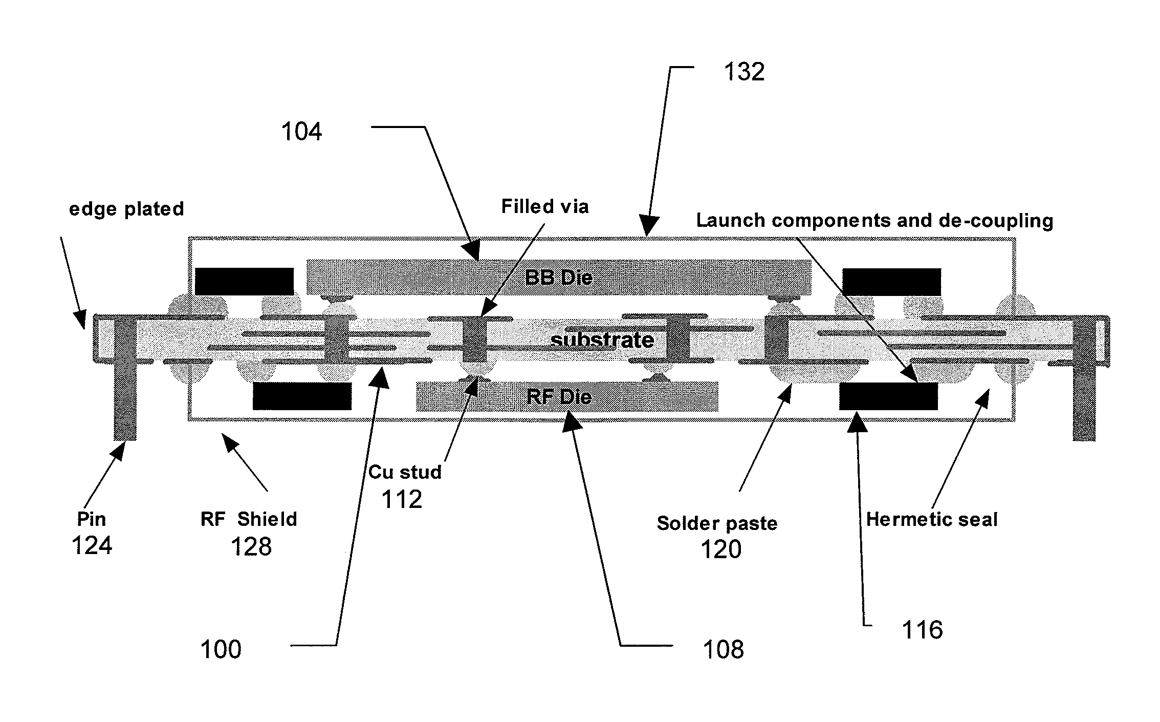
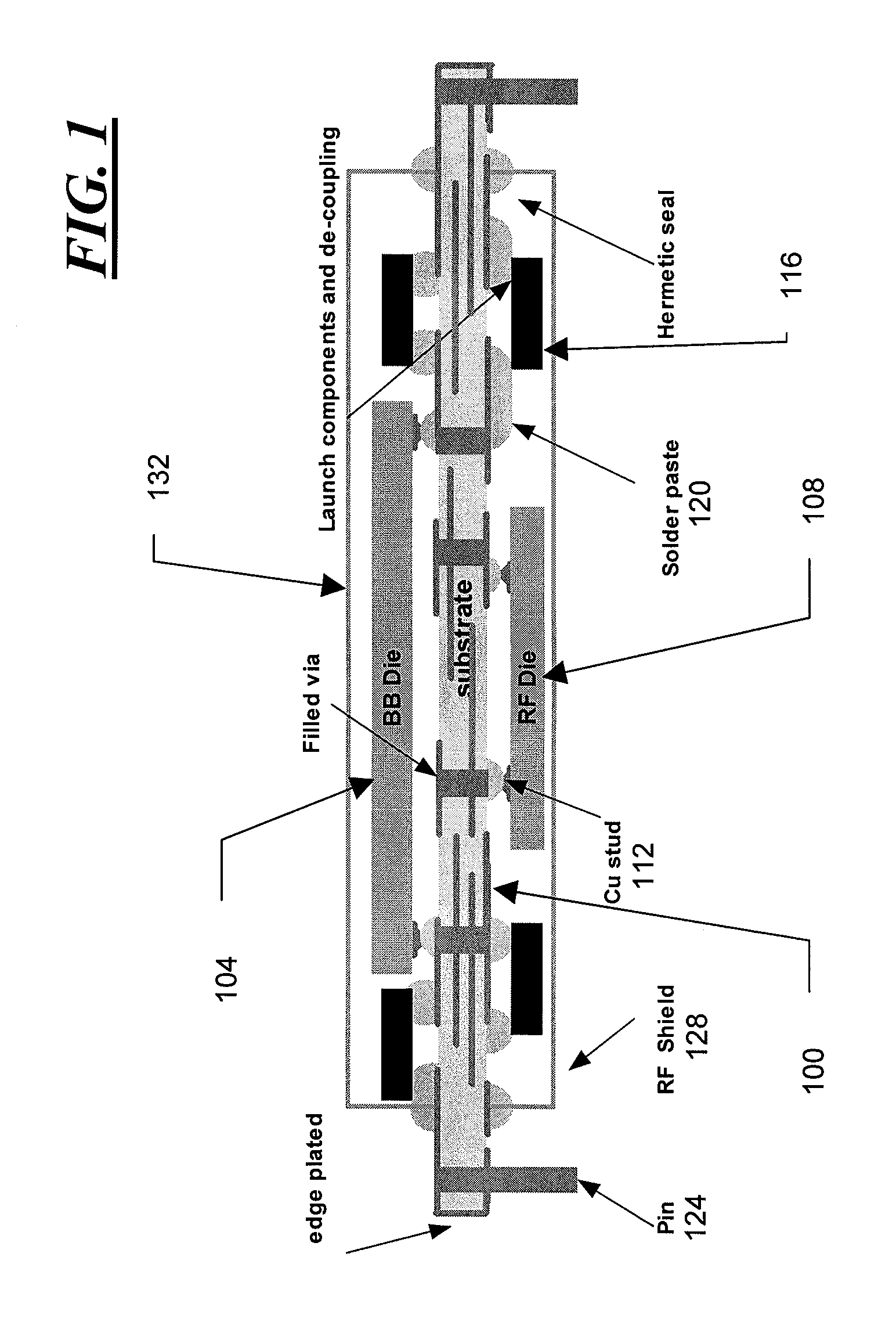
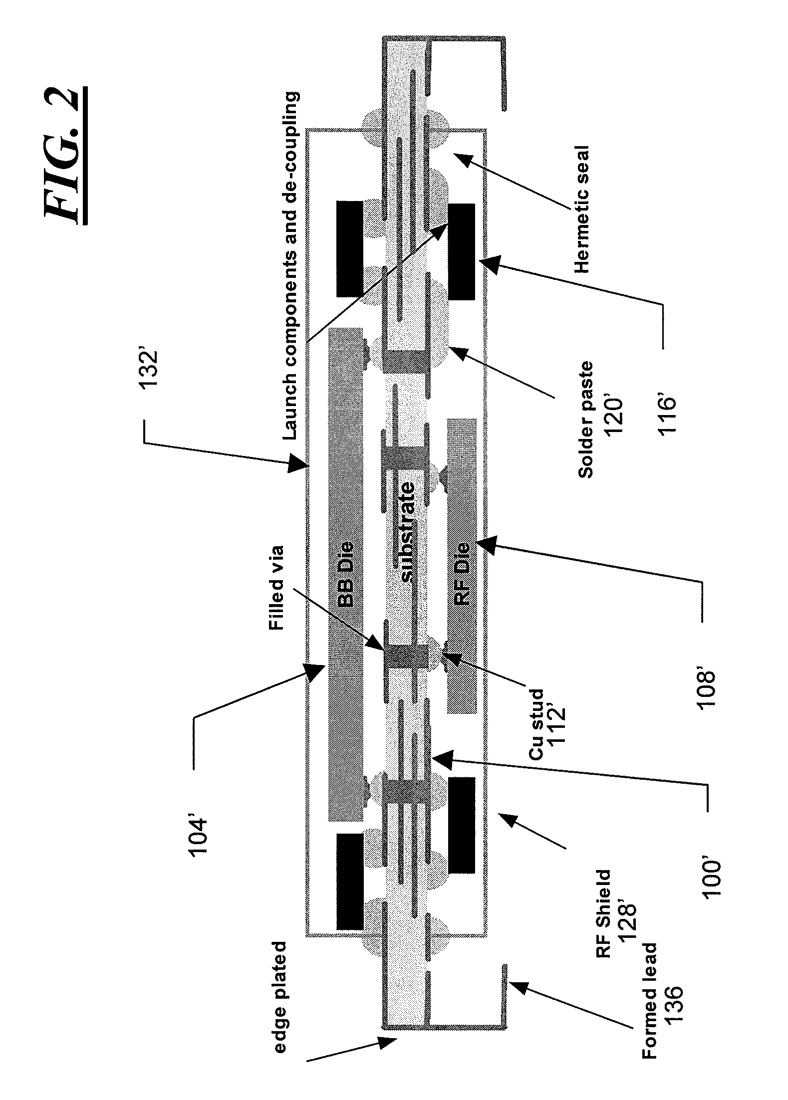
[0030]With reference to FIG. 1, one embodiment of the present invention provides an MCM using a multilayer substrate 100 to provide electrical connections as well as an electrical shielding between a baseband die 104 and a radio-frequency die 108. The copper bumps 112 are connected to the pads of dies 104 and 108 to facilitate the attachment of the dies 104, 108 to the substrate 100 Solder paste 120 is applied to the particular areas of the substrate 100 corresponding to the bumps 112 and contacts of discrete components 116 to be included in the package and heated until it melts, forming electrical connections between the dies 104, 108 and components 116 and the substrate 100.

[0031]Although the multilayer substrate 100 potentially provides better shielding between the baseband die 104 and the radio frequency di...


PUM


Abstract

Methods and apparatus for multichip modules having improved shielding and isolation properties.

Description

CROSS-REFERENCE TO RELATED APPLICATIONS[0001]This application claims the benefit of U.S. Provisional Patent Application No. 60 / 875,972, filed on Dec. 20, 2006, which is hereby incorporated by reference as if set forth herein in its entirety.FIELD OF THE INVENTION[0002]The present invention relates to methods and apparatus for the packaging of integrated circuits, and in particular to the packaging of a plurality of integrated circuits in a module.BACKGROUND OF THE INVENTION[0003]Modern electronic devices typically include one or more integrated circuits (ICs). In order to operate, each integrated circuit must have electrical connections to other components, such as a power supply. This is typically achieved through the use of a package surrounding the integrated circuit and one or more solder bonds or pin-and-socket connections to join the package to a substrate.[0004]The package is often disproportionately large relative to the integrated circuit that it contains, and size reductio...

Claims


Application Information

Patent Timeline
Patent Type & Authority Applications(United States)
IPC IPC(8): H01L23/498H01L21/98
CPCH01L23/552H01L2224/16235H01L2223/6688H01L2224/16H01L2924/15312H01L2924/16152H01L2924/19105H01L2924/3025H05K1/0218H05K1/141H05K1/144H05K1/182H05K1/183H05K3/3442H05K2201/045H05K2201/09072H05K2201/09618H05K2201/10371H05K2201/2018H05K2203/1572H01L25/16H01L2924/00011H01L2924/00014H01L2924/1627H01L2224/0401
Inventor NUYTKENS, PETER R.HAWAT, NOUREDDINEKULINETS, JOSEPH M.
Owner CUSTOM ONE DESIGN
Why Eureka
Try Eureka