Addressable hierarchical metal wire test methodology

a hierarchical metal wire and test methodology technology, applied in semiconductor/solid-state device testing/measurement, semiconductor/solid-state device details, instruments, etc., can solve problems such as forming voids in metal, em problems becoming worse, and feature sizes both in width and thickness of metal wires further scaled

Inactive Publication Date: 2008-07-03
GLOBALFOUNDRIES INC
View PDF34 Cites 14 Cited by
  • Summary
  • Abstract
  • Description
  • Claims
  • Application Information

AI Technical Summary

Benefits of technology

[0017]In view of the foregoing and other exemplary problems, drawbacks, and disadvantages of the conventional methods and structures, an exemplary feature of the present invention is to provide a method and structure in which a low-cost, fast turn-around metal test structure which is formed by using only BEOL metal wiring levels.
[0019]Accordingly, the present invention provides a low-cost, fast turn-around metal test structure which is formed by using only BEOL metal wiring level. Furthermore, the present invention provides a defect addressable test macro and a corresponding test algorithm. Additionally, the present invention is useful for high-speed automatic testing tools using test programs.

Problems solved by technology

In short, electro-migration failure is caused by a positive divergence of the ionic flux leads to an accumulation of vacancies, forming void in the metal.
The EM problem becomes worse as the feature sizes both in width and thickness of metal wirings are further scaled.
Furthermore, it requires a poly-silicon layer, which means more process steps and is thus more expensive to make the test macro.
It cannot, however, position the open / short defect location, nor can it count the number of defects in the test macro.
Therefore, this method provides very little information about the metal defects.
For such design, however, it is not possible to provide defect locations.
However, all the conventional test methodologies proposed so far can not provide open / short defect address.
They may be used to qualify the BEOL process, but it will not be easy for the engineer to spot the defect and zoom in to conduct failure analysis.

Method used


Image

  • Addressable hierarchical metal wire test methodology
  • Addressable hierarchical metal wire test methodology
  • Addressable hierarchical metal wire test methodology

Examples


Embodiment Construction

[0026]Referring now to the drawings, and more particularly to FIGS. 1-4C, there are shown exemplary embodiments of the method and structures according to the present invention.

[0027]The present invention doesn't attempt to replace the existing TDDB or EM testing methodology. It is important to continue conduct wafer level tests, qualification tests and burn-in test to out stress the bad chips.

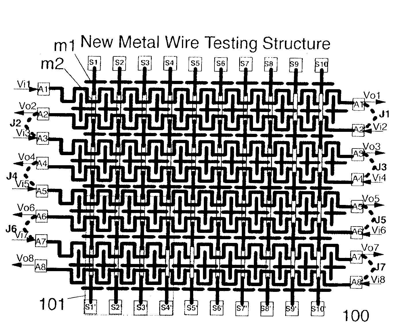
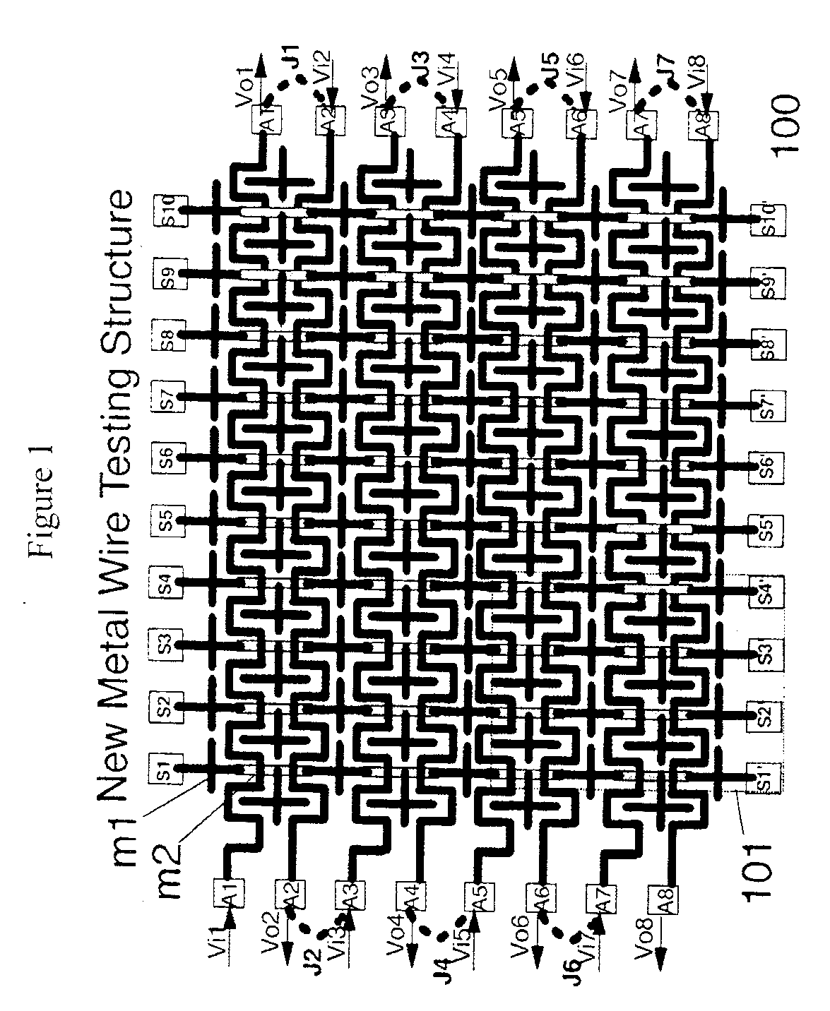
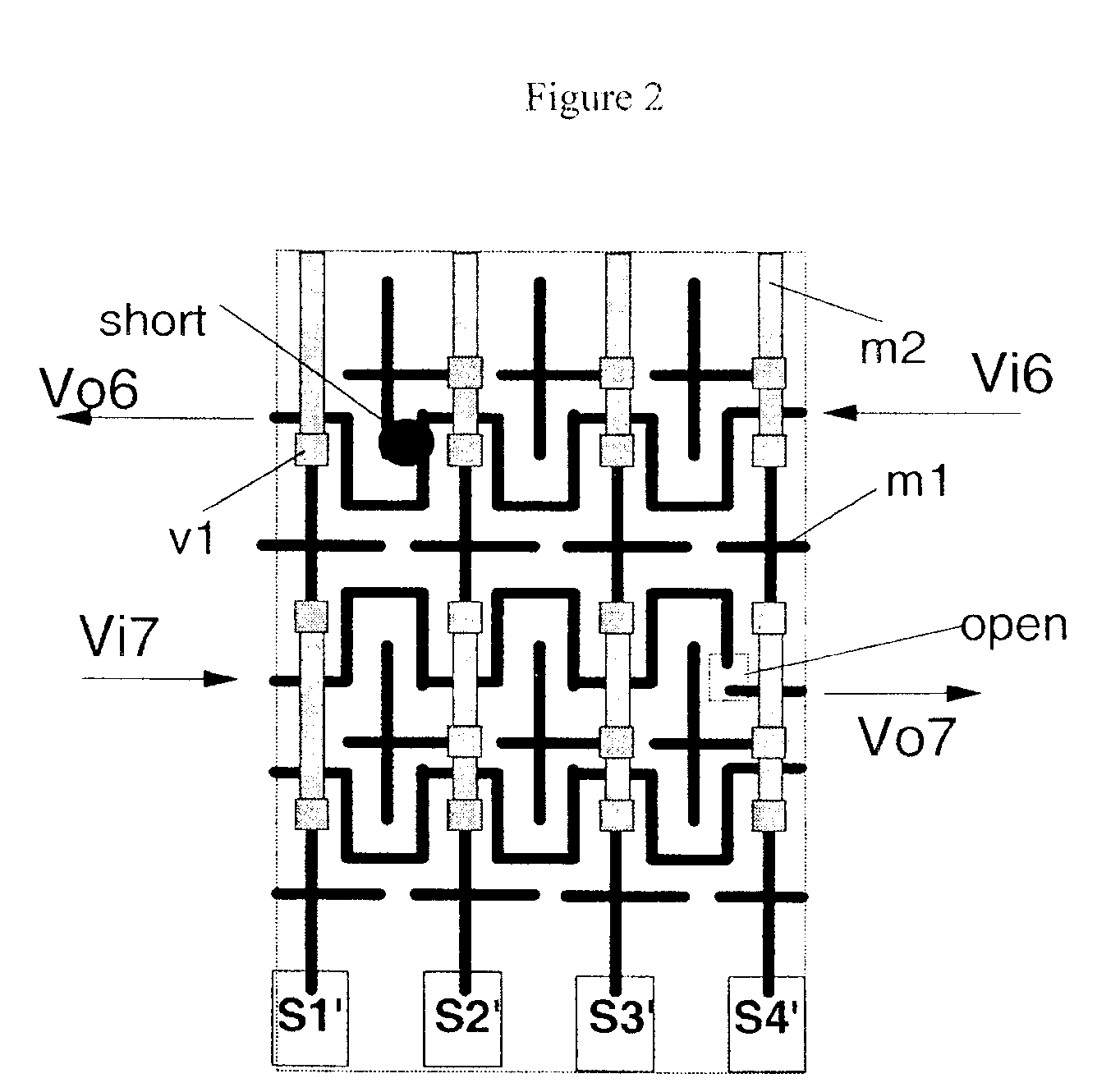
[0028]An example of the addressable wiring test array (or AWTA) 100 is shown in FIG. 1. A plurality of metal wiring is laid-out in the horizontal direction with or without turns. Each metal wiring can be tested individually with corresponding probe pads. Based on the same principle, it is conceivable that more than one horizontal wire can be joined at the end to have a “u” turn in order to reduce the number of the pads. In between two adjacent metal wirings, segmented probing wirings are presented. A plurality of segmented probing wiring is connected in the vertical direction via next metal lev...


PUM


Abstract

A method of monitoring and testing electro-migration and time dependent dielectric breakdown includes forming an addressable wiring test array, which includes a plurality or horizontally disposed metal wiring and a plurality of segmented, vertically disposed probing wiring, performing a single row continuity / resistance check to determine which row of said metal wiring is open, performing a full serpentine continuity / resistance check, and determining a position of short defects.

Description

BACKGROUND OF THE INVENTION[0001]1. Field of the Invention[0002]The present invention generally relates to a method and apparatus for monitoring and testing electro-migration (EM) and time dependent dielectric breakdown (TDDB), and more particularly to a method and apparatus for addressable wiring test array formed using only back-end-of-the-line (BEOL) metal wiring levels.[0003]2. Description of the Related Art[0004]Generally, two types of tests are conducted on the metal wiring of a chip. The first one is called TDDB (time dependent dielectric breakdown), and the second one is the EM (electro-migration) test.[0005]The purpose of TDDB test is to find out whether the quality of the insulator used for the BEOL (back-end-of-the-line) meets specifications. This test is done by stressing metal wiring in the BEOL at different voltages. One example is to apply a voltage ranged between 5 and 35 volts on the testing metal wire and the adjacent probing metal wire. The time required for elect...

Claims


Application Information

Patent Timeline
Patent Type & Authority Applications(United States)
IPC IPC(8): H01L21/66G01R31/26
CPCG01R31/2858H01L22/14H01L2924/0002Y10S438/927H01L2924/00
Inventor CHANDA, KAUSHIKCLEVENGER, LAWRENCEDALTON, TIMOTHY J.HSU, LOUIS L. C.YANG, CHIH-CHAO
Owner GLOBALFOUNDRIES INC
Why Eureka
Try Eureka