
Method of manufacture for a semiconductor device

Active Publication Date: 2008-07-10
MAXPOWER SEMICON INC
View PDF36 Cites 61 Cited by
  • Summary
  • Abstract
  • Description
  • Claims
  • Application Information

AI Technical Summary

Benefits of technology

[0028]Numerous benefits are achieved using the present invention over conventional techniques. For example, in an embodiment according to the present invention, improved MOSFET conduction and switching performance is achieved. Moreover, in other embodiments, paralleling of alternate charge balanced dielectric and silicon layers provides a device with performance exceeding the one dimensional silicon breakdown voltage limit for a given doping concentration. The use of fixed charge reduces the capacitances compared to conventional techniqu

Problems solved by technology

In a SJ structure, the minimum widths of the n-type and p-type pillars set a limitation on reducing cell pitch and scaling the device.
There are also several

Method used


Image

  • Method of manufacture for a semiconductor device
  • Method of manufacture for a semiconductor device
  • Method of manufacture for a semiconductor device

Examples


Embodiment Construction

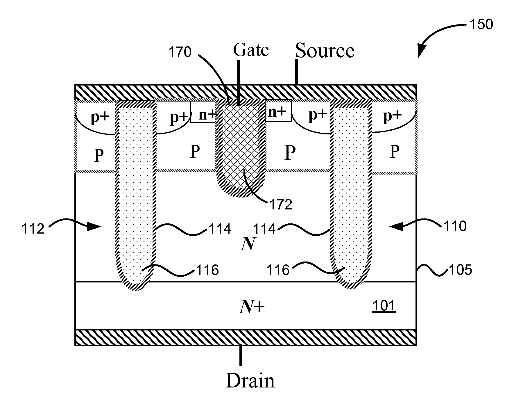
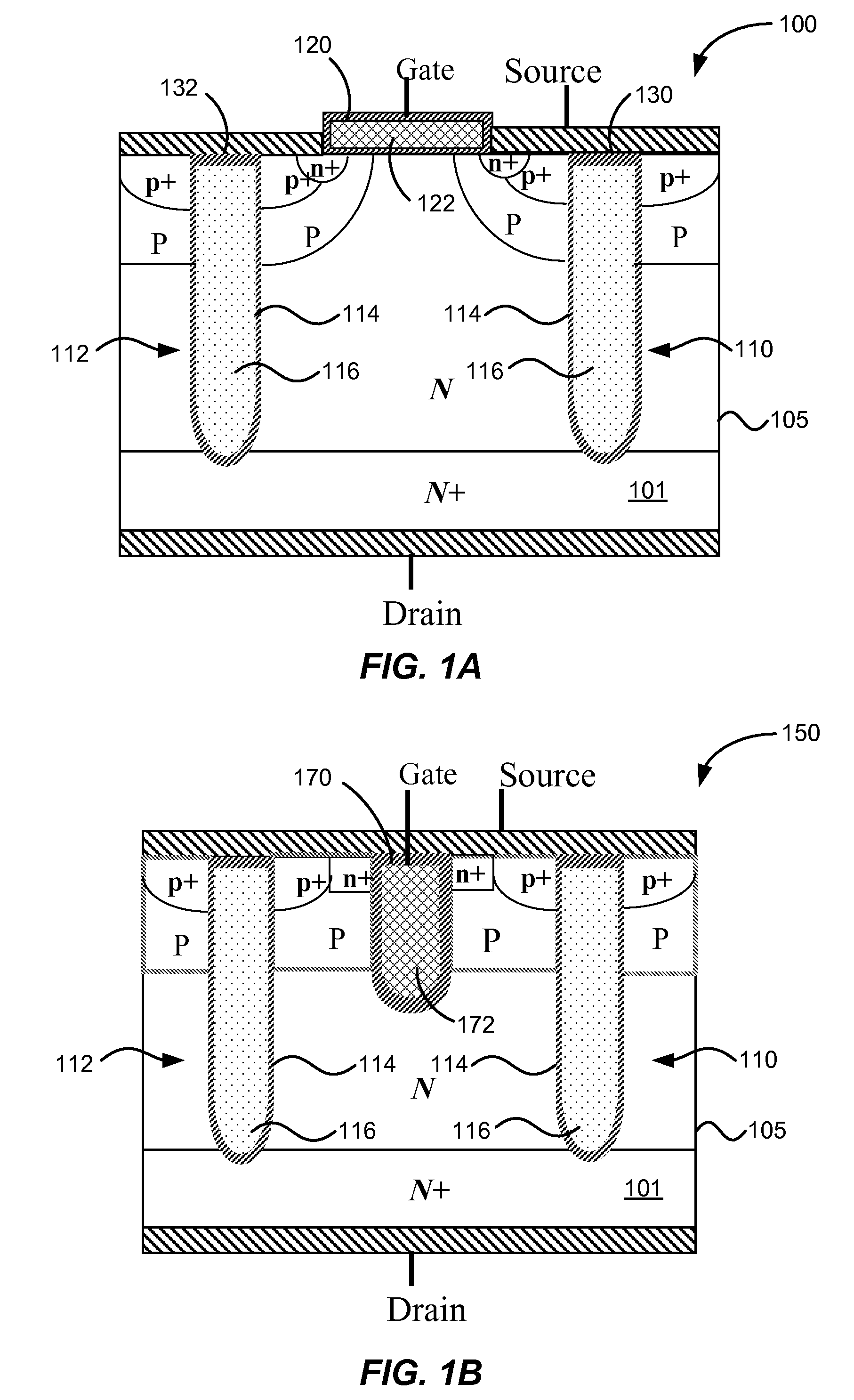
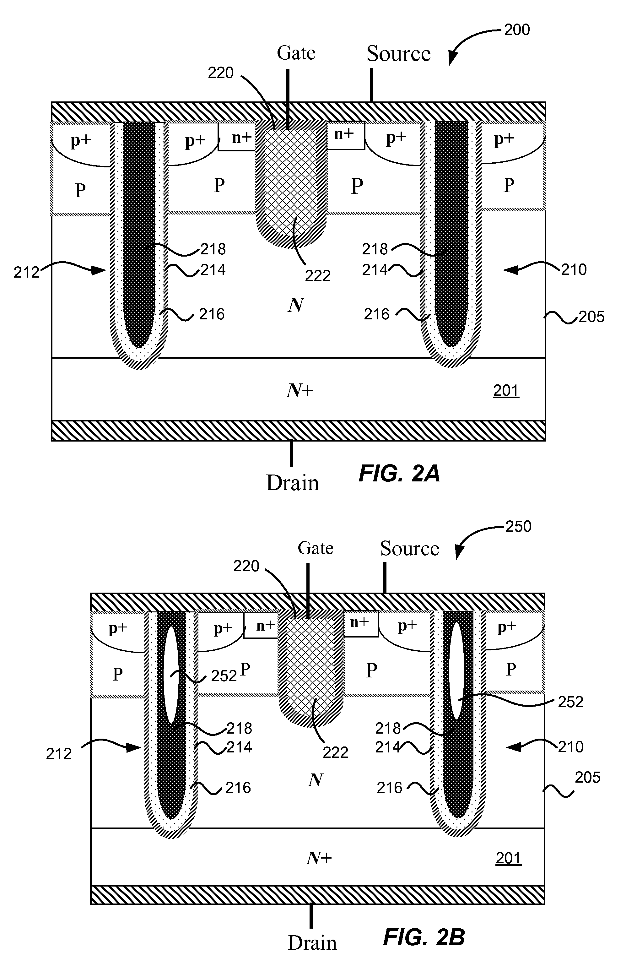
[0118]According to embodiments of the present invention, a power MOSFET structure is provided that is characterized by improved conduction and switching performance. In a particular embodiment, a high voltage MOSFET structure is provided in which dielectric layers containing charge are used to balance the charge in the drift region. By alternating dielectric and silicon layers that are charge balanced, the structure's performance exceeds the one dimensional silicon breakdown voltage limit for a given doping concentration. Both vertical and lateral MOSFET structures are provided by embodiments of the present invention. Furthermore, in a specific embodiment, a lateral structure is used in which dielectric layers with charge are combined with double or multiple Reduced SURface Field (Resurf) techniques for additional improvement in breakdown voltage and / or on-resistance. Methods of fabricating these structures are described and further details, embodiments and examples of the invention...


PUM


Abstract

A method of manufacturing a semiconductor device includes providing a semiconductor layer of a first conductivity type and forming a semiconductor layer of a second conductivity type thereon. The method also includes forming an insulator layer on the semiconductor layer of the second conductivity type, etching a trench into at least the semiconductor layer of the second conductivity type, and forming a thermal oxide layer in the trench and on the semiconductor layer of the second conductivity type. The method further includes implanting ions into the thermal oxide layer, forming a second insulator layer, removing the second insulator layer from a portion of the trench, and forming an oxide layer in the trench and on the epitaxial layer. Moreover, the method includes forming a material in the trench, forming a second gate oxide layer over the material, and patterning the second gate oxide layer.

Description

CROSS-REFERENCES TO RELATED APPLICATIONS[0001]The present application claims benefit under 35 U.S.C. § 119(e) of U.S. Provisional Patent Application No. 60 / 879,434, filed Jan. 9, 2007, entitled “Power MOS Transistor,” the disclosure of which is incorporated herein by reference in its entirety.[0002]The present application is related to co-pending and commonly assigned U.S. patent application Ser. No. 11 / 971,096, filed on Jan. 8, 2008, entitled “Semiconductor device,” the disclosure of which is hereby incorporated by reference for all purposes.[0003]The following four regular U.S. patent applications (including this one) are being filed concurrently, and the entire disclosure of the other applications are incorporated by reference into this application for all purposes:[0004]Application Ser. No. ______, filed Jan. 8, 2008, entitled “Semiconductor device” (Attorney Docket No. 027049-000210US);[0005]Application Ser. No. ______, filed Jan. 8, 2008, entitled “Semiconductor device” (Attor...

Claims


Application Information

Patent Timeline
IPC IPC(8): H01L21/336
CPCH01L21/26586H01L29/66666H01L29/0619H01L29/0634H01L29/0653H01L29/0661H01L29/0692H01L29/0696H01L29/0847H01L29/0878H01L29/1095H01L29/408H01L29/4236H01L29/42368H01L29/66734H01L29/7802H01L29/7809H01L29/7811H01L29/7813H01L29/7827H01L29/7835H01L21/2003H01L21/28008H01L21/2658H01L29/66537H01L21/823885H01L21/02164H01L21/0217H01L21/02321H01L21/265H01L21/30604H01L21/324H01L21/76224H01L29/0649
Inventor DARWISH, MOHAMED N.
Owner MAXPOWER SEMICON INC
Features
  • Generate Ideas
  • Intellectual Property
  • Life Sciences
  • Materials
  • Tech Scout
  • Unparalleled Data Quality
  • Higher Quality Content
  • 60% Fewer Hallucinations
Learn More